The quest for efficient, lossless energy transmission has taken a significant leap forward as researchers at Chalmers University of Technology in Sweden have pioneered a method to stabilize superconductivity at higher temperatures and under intense magnetic pressure. By shifting the focus from the internal chemical composition of superconducting materials to the physical architecture of the surfaces upon which they are grown, the team has addressed two of the most persistent bottlenecks in condensed matter physics. This development, published in the journal Nature Communications, provides a potential blueprint for a new generation of electronics that could drastically reduce the global energy footprint of the information and communications technology (ICT) sector.
Superconductivity, a state in which a material conducts electricity with zero resistance and expels magnetic fields, has long been viewed as the "holy grail" of power engineering. However, the phenomenon typically manifests only under conditions of extreme cold or high pressure, environments that are difficult and expensive to maintain outside of specialized laboratory settings. The Chalmers breakthrough suggests that by "sculpting" the substrate—the foundation layer—on a nanoscopic scale, it is possible to influence the electronic behavior of the superconducting film, making it more resilient to the environmental factors that usually destroy the superconducting state.
The Energy Crisis and the Superconductivity Solution
The urgency of this research is underscored by the staggering energy demands of the modern digital age. Recent data suggests that the global ICT infrastructure, including massive data centers, cellular networks, and personal computing devices, now accounts for between 6 and 12 percent of total global electricity consumption. As artificial intelligence, cloud computing, and the Internet of Things (IoT) continue to expand, these figures are projected to rise sharply.
Conventional electronic systems operate on the principle of semiconducting and metallic conduction, which inherently involves resistance. This resistance converts a portion of the electrical energy into heat, a phenomenon known as Joule heating. In large-scale operations like data centers, this creates a double-sided energy drain: electricity is lost during processing, and further electricity must be spent on high-powered cooling systems to prevent hardware from melting. Superconductors offer a theoretical exit from this cycle. Because they allow electrons to flow without friction, they generate no heat. If integrated into the global power grid and consumer electronics, they could theoretically make these systems hundreds of times more efficient, potentially saving trillions of kilowatt-hours annually.
Historical Challenges: Temperature and Magnetism
Since the discovery of superconductivity in mercury by Heike Kamerlingh Onnes in 1911, the field has struggled with the "critical temperature" (Tc) problem. Early superconductors required liquid helium to reach temperatures near absolute zero (minus 273 degrees Celsius). The discovery of "high-temperature" superconductors (HTS) in the 1980s—specifically the cuprate family—was a turning point, as these materials could function at temperatures reachable with liquid nitrogen (roughly minus 196 degrees Celsius). While liquid nitrogen is cheaper and easier to handle than liquid helium, it still requires heavy insulation and refrigeration.
Beyond temperature, magnetic fields represent a second major hurdle. When a superconductor is exposed to a magnetic field above a certain threshold, the field penetrates the material, creating vortices that disrupt the flow of electrons and eventually "quench" the superconducting state. This is particularly problematic for applications like Magnetic Resonance Imaging (MRI), particle accelerators, and quantum computers, all of which utilize or generate powerful magnetic fields. Finding a way to maintain superconductivity in the presence of these fields is essential for moving the technology from the lab to the marketplace.
A Paradigm Shift in Engineering: Sculpting the Substrate
The research team at Chalmers, led by Floriana Lombardi, Professor of Quantum Device Physics, departed from the traditional method of chemical doping. In most previous studies, scientists attempted to raise the critical temperature by adding or removing atoms within the superconducting material’s crystal lattice. While effective to a point, this process often destabilizes the material’s structural integrity or makes it brittle.
The Chalmers team instead focused on the interface between the superconductor and its supporting substrate. They utilized a cuprate material—Yttrium Barium Copper Oxide (YBCO)—and deposited it in a layer only a few nanometers thick. This thickness is approximately one-millionth the width of a human hair. At such a scale, the material is highly sensitive to the topography of the surface it rests upon.
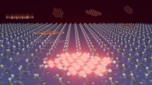
"By sculpting the surface that the superconductor rests on, we were able to induce superconductivity at significantly higher temperatures than previously possible," Lombardi stated. The researchers prepared the substrate—typically a crystalline material like strontium titanate—by heating it in a vacuum to extreme temperatures. This process caused the surface of the substrate to reorganize into a series of "nanofacets," characterized by a rhythmic pattern of microscopic ridges and valleys.
Mechanisms of Interfacial Stabilization
When the YBCO film was grown atop this nanofaceted surface, the atoms in the superconducting layer were forced to align with the pre-existing pattern of the substrate. This structural "guidance" created a unique electronic environment at the interface. The researchers observed that the electrons in the YBCO layer began to exhibit a "preferential direction," a phenomenon that helped stabilize the superconducting state against thermal fluctuations.
Eric Wahlberg, a researcher at RISE Research Institutes of Sweden and a key contributor to the study, noted that the atomic arrangement of the substrate acts as a template. "By changing the surface design of the substrate, we were able to influence the superconducting properties and ensure they were preserved, even at higher temperatures and when high magnetic fields were applied," Wahlberg explained.
Perhaps the most significant finding was the material’s newfound resistance to magnetic fields. In typical thin-film superconductors, magnetic fields can easily penetrate and disrupt the electron pairs (Cooper pairs) responsible for superconductivity. However, the nanofaceted structure created by the Chalmers team appeared to "pin" the magnetic flux lines, preventing them from moving and dissipating energy. This allows the material to remain superconducting in magnetic environments that would normally render it useless.
Chronology of the Research and International Collaboration
The breakthrough is the result of several years of incremental progress in nanofabrication and thin-film physics. The project involved an international consortium of scientists, reflecting the global interest in solving the superconductivity puzzle.
The timeline of the research began with the development of precise vacuum-annealing techniques at the Myfab Chalmers cleanroom facility. Following the initial substrate preparation, the team moved to the growth of the ultrathin YBCO films using pulsed laser deposition. The subsequent testing phase required high-precision measurements of electrical resistance and magnetic susceptibility across a wide range of temperatures and field strengths.
The study, "Boosting superconductivity in ultrathin YBa2Cu3O7−δ films via nanofaceted substrates," brought together experts from:
- Chalmers University of Technology (Sweden)
- RISE Research Institutes of Sweden
- Ca’ Foscari University of Venice (Italy)
- Birla Institute of Technology and Science – Pilani (India)
- Indian Institute of Science Education and Research (IISER)
- Uppsala University (Sweden)
- Université Grenoble Alpes and Université de Toulouse (France)
- BTU Cottbus-Senftenberg (Germany)
The project was supported by significant funding from the Swedish Research Council (VR), the Knut and Alice Wallenberg Foundation, and the European Union through an EIC Pathfinder grant. This level of institutional support highlights the strategic importance of superconductivity in the future of European and global technology.
Broader Implications for Quantum Computing and Energy
The implications of this research extend far beyond more efficient power lines. One of the most immediate beneficiaries could be the field of quantum computing. Quantum processors rely on superconducting circuits, such as SQUIDs (Superconducting Quantum Interference Devices) and qubits, to process information. These components are notoriously fragile and must be kept at temperatures near absolute zero to function. By increasing the temperature threshold and magnetic field resilience of these components, the Chalmers approach could lead to more robust quantum computers that require less cumbersome cooling infrastructure.
In the energy sector, the ability to create thin-film superconductors that can withstand magnetic fields opens the door to more powerful and compact Maglev (magnetic levitation) trains and advanced fusion energy reactors. Fusion reactors, which attempt to replicate the energy production of the sun, require incredibly strong magnetic fields to confine plasma. Current superconducting magnets for fusion are massive and require cooling to 4 Kelvin (-269°C). Enhancing the performance of superconductors at higher temperatures could significantly reduce the cost and complexity of these "star-in-a-jar" energy projects.
Furthermore, the "substrate engineering" principle introduces a new design philosophy for materials science. Rather than looking for a single "miracle material," engineers can now look at the synergy between different layers of a device. This "interfacial engineering" could be applied to other classes of materials, such as topological insulators or ferroelectrics, potentially leading to breakthroughs in sensors, medical imaging, and telecommunications.
Conclusion and Future Outlook
While room-temperature superconductivity remains the ultimate goal, the Chalmers University study provides a tangible path forward by optimizing existing high-temperature superconductors through nanostructural design. The transition from chemical manipulation to geometric sculpting represents a maturation of the field, moving from trial-and-error chemistry to precise nanoscale engineering.
"This shows that very small changes at the nanoscale can have decisive effects and may even unlock the full potential of superconductivity in future electronics," Professor Lombardi concluded. As the researchers look toward the next phase of their work, the focus will likely shift to scaling these nanofaceted substrates for industrial production. If successful, the ridges and valleys of a microscopic surface may eventually pave the way for a global energy revolution, transforming the way we power our world and the machines that inhabit it.