In a significant leap toward making quantum technologies more accessible and scalable, researchers at Stanford University have engineered a nanoscale optical device capable of functioning at room temperature while facilitating a robust link between the quantum properties of light and electrons. This breakthrough addresses one of the most persistent hurdles in the field of quantum science: the requirement for extreme cryogenic cooling. By eliminating the need for temperatures approaching absolute zero—approximately -459 degrees Fahrenheit—this new device paves the way for a generation of smaller, cost-effective quantum systems that can transmit information across vast distances using existing infrastructure.
The research, recently published in the journal Nature Communications, details a mechanism that enables entanglement between photons and electrons. Entanglement, a phenomenon Albert Einstein famously described as "spooky action at a distance," is the fundamental requirement for quantum communication. It allows particles to remain interconnected such that the state of one instantly influences the state of the other, regardless of the distance separating them. Until now, maintaining this delicate connection usually required massive, energy-intensive dilution refrigerators to prevent thermal noise from disrupting the quantum states, a process known as decoherence.
The Challenge of Quantum Decoherence and Cryogenics
To understand the magnitude of the Stanford team’s achievement, one must consider the current state of quantum infrastructure. Modern quantum computers, such as those developed by IBM, Google, and Rigetti, rely primarily on superconducting qubits. These systems must be kept at temperatures colder than outer space to function. The cost of the specialized cooling equipment alone can reach hundreds of thousands of dollars, and the electricity required to maintain these temperatures is substantial.
When a quantum system is exposed to heat, the atoms and electrons begin to vibrate and interact with their environment. This interaction causes the "spin" of an electron—a property used to store quantum information—to flip or randomize almost instantly. This loss of information, or decoherence, has been the primary barrier to moving quantum technology out of specialized laboratories and into the commercial sector. The Stanford device overcomes this by utilizing a unique combination of materials and light manipulation that stabilizes these states even at 70 degrees Fahrenheit.
Engineering "Twisted Light" at the Nanoscale
The device’s functionality relies on a sophisticated marriage of two components: a thin layer of molybdenum diselenide (MoSe2) and a nanopatterned silicon substrate. Molybdenum diselenide is a member of the transition metal dichalcogenide (TMDC) family, a class of "2D materials" that are only a few atoms thick. These materials are highly prized by physicists for their exceptional optical properties and their ability to host stable quantum states.
The innovation lies in how the silicon substrate is shaped. The Stanford team used advanced nanofabrication techniques to etch the silicon with patterns that are smaller than the wavelength of visible light. When light passes through these structures, it is transformed into what the researchers call "twisted light."
"The silicon nanostructures enable what we call ‘twisted light,’" explained Feng Pan, a postdoctoral scholar in the Dionne lab and the paper’s lead author. "The photons spin in a corkscrew fashion, but more importantly, we can use these spinning photons to impart spin on electrons that are the heart of quantum computing."
By controlling the angular momentum of the photons—essentially making them spiral in a specific direction—the researchers can "write" information onto the electrons within the MoSe2 layer. This process creates a stable spin connection between the light and the matter, providing the theoretical and practical basis for a quantum bridge.
The Role of Transition Metal Dichalcogenides (TMDCs)
The selection of molybdenum diselenide was not accidental. Jennifer Dionne, a professor of materials science and engineering at Stanford and the study’s senior author, noted that while the material itself has been studied for years, the specific application in this device represents a new frontier. TMDCs are unique because they allow for strong light-matter interactions. In most materials, light passes through or reflects off the surface with minimal impact on the internal electronic states. In MoSe2, however, the "twisted" photons are efficiently absorbed and coupled to the electron spins.
The collaboration involved several Stanford experts, including Fang Liu and Tony Heinz, who provided deep insights into the behavior of 2D materials. Their combined expertise allowed the team to solve a critical problem: typically, electrons in these materials lose their spin orientation too quickly to be useful for data transmission. By confining the light within the silicon nanostructures, the researchers were able to enhance the coupling effect, effectively "shielding" the electron spin from the thermal vibrations of the room-temperature environment.
Implications for the Quantum Internet
The ability to link photons and electrons at room temperature is a cornerstone for the development of a "Quantum Internet." While classical fiber-optic networks transmit data using pulses of light representing ones and zeros, a quantum network would transmit qubits. Qubits can exist in multiple states simultaneously (superposition), allowing for exponentially more complex calculations and virtually unhackable communication through Quantum Key Distribution (QKD).
Current quantum networking experiments often require bulky "repeaters" that must be kept frozen to preserve the signal. The Stanford device’s compact, room-temperature design suggests that future quantum repeaters could be significantly smaller and integrated into existing telecommunications hubs. This would drastically reduce the capital expenditure required to build a global quantum-secure network.
Furthermore, the device’s reliance on silicon—the same material used in traditional computer chips—means that it could potentially be manufactured using existing semiconductor fabrication processes. This compatibility with the current tech ecosystem is a major advantage over more exotic quantum platforms that require entirely new manufacturing paradigms.
Comparative Analysis: A Shift in Quantum Hardware
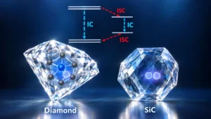
The Stanford approach represents a departure from other leading methods of room-temperature quantum research. For instance, some researchers use "nitrogen-vacancy centers" in diamonds to achieve room-temperature quantum states. While effective, the process of creating and placing these diamond defects is difficult to scale. Others explore trapped ions, which require complex laser arrays and vacuum chambers.
In contrast, the Stanford device is a solid-state optical system. It is passive, meaning it does not require an external power source to maintain the nanostructure’s properties; it simply requires the input of light. This simplicity makes it a candidate for integration into a wide range of devices, from satellites to mobile hardware.
Economic and Industrial Impact
The move toward room-temperature quantum systems is expected to accelerate the commercialization of quantum sensors and AI. In the field of sensing, quantum devices can detect minute changes in magnetic fields or gravity, which has applications in medical imaging and mineral exploration. In the realm of artificial intelligence, quantum-enhanced processors could handle the massive datasets required for training large language models far more efficiently than current GPUs.
Industry analysts suggest that the quantum computing market, currently valued in the hundreds of millions, could grow to over $100 billion by the 2030s if hardware hurdles like cooling are resolved. The Stanford research directly addresses the "operating cost" variable in that economic equation. By removing the need for liquid helium—a finite and increasingly expensive resource used in cryogenics—the researchers have made the technology more sustainable.
Chronology of Development and Future Roadmap
The development of this device is the result of several years of interdisciplinary research at Stanford’s Precourt Institute for Energy and the Stanford Nano Shared Facilities. The project began with theoretical modeling of how light interacts with 2D materials, followed by the design of the silicon "metasurfaces" (the patterned layers).
Moving forward, the team is exploring other TMDC materials, such as tungsten diselenide (WSe2), to see if they can achieve even longer spin-coherence times. They are also working on integrating the device with other essential quantum components, such as single-photon detectors and modulators.
While the results are promising, the researchers are realistic about the timeline for consumer applications. "If we can do that, maybe someday we could do quantum computing in a cell phone," Feng Pan said. "But that’s a 10-plus-year plan."
The next five years will likely focus on laboratory-scale quantum networks and specialized industrial sensors. The integration of these nanoscale devices into larger systems will require rigorous testing to ensure that the entanglement remains stable over kilometers of fiber-optic cable.
Conclusion: A Step Toward Practical Quantum Utility
The work led by Jennifer Dionne and Feng Pan marks a pivotal moment in the transition from theoretical quantum physics to practical quantum engineering. By demonstrating that the fundamental building blocks of quantum communication—photon-electron entanglement—can be achieved and maintained at room temperature on a silicon-based platform, the Stanford team has lowered the barrier to entry for the next technological revolution.
As the global race for quantum supremacy continues, the focus is shifting from simply building more qubits to building usable and deployable qubits. This nanoscale device, invisible to the human eye but powerful in its manipulation of the subatomic world, represents a significant stride toward a future where quantum power is not confined to the laboratory but is integrated into the fabric of everyday digital life.