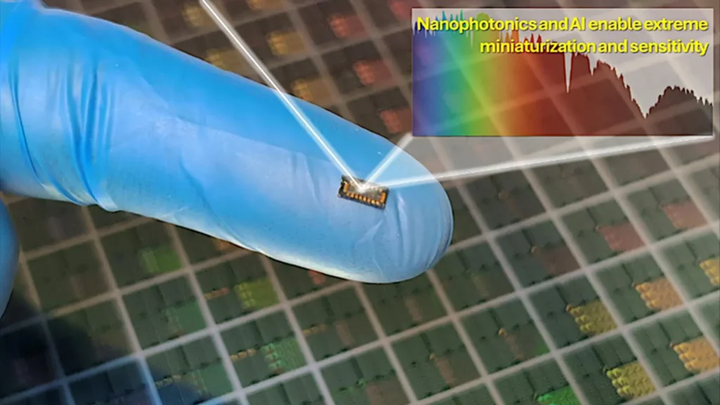
The field of optical sensing has reached a significant milestone as researchers at the University of California, Davis (UC Davis) have successfully miniaturized the complex mechanics of a laboratory-grade spectrometer into a single silicon chip. This breakthrough, recently detailed in the journal Advanced Photonics, represents a departure from nearly two centuries of optical design. By replacing bulky physical components with a combination of advanced nanostructuring and artificial intelligence, the team has produced a device that measures just 0.4 square millimeters. This innovation effectively reduces a piece of equipment that typically occupies a desktop to a footprint smaller than a grain of sand, promising to bring high-resolution chemical analysis to consumer electronics and wearable medical devices.
Spectrometers are essential tools in modern science, used to identify the chemical composition of substances by analyzing how they interact with light. Every material possesses a unique "spectral fingerprint"—a specific pattern of light absorption and reflection across different wavelengths. Historically, capturing this fingerprint required a series of mirrors, prisms, or gratings to physically disperse light into a rainbow, which was then projected onto a sensor. Because the light must travel a specific distance to achieve adequate separation of colors, these devices have remained stubbornly large. The UC Davis team’s "spectrometer-on-a-chip" bypasses this physical requirement entirely, using computational power to reconstruct light profiles that would otherwise be impossible to detect at such a small scale.
The Evolution of Spectroscopy: From Newton to the Nanoscale
To understand the magnitude of this achievement, one must consider the historical trajectory of spectral analysis. In the 1660s, Sir Isaac Newton first demonstrated that white light could be split into a spectrum using a glass prism. For the next 300 years, the fundamental principle remained the same: use geometry and distance to separate wavelengths. By the mid-20th century, the advent of electronic detectors allowed for more precise measurements, leading to the development of the high-performance spectrometers used today in pharmaceuticals, forensic science, and astronomy.
However, the "miniaturization wall" became a significant hurdle in the 21st century. While sensors and processors have shrunk according to Moore’s Law, the physics of light refraction did not scale as easily. Previous attempts to create portable spectrometers often resulted in a significant loss of resolution or a limited spectral range. The UC Davis research team sought to overcome this by reimagining the sensor itself. Instead of asking how to shrink a prism, they asked how to extract spectral data from light without dispersing it first. This shift from physical optics to computational optics marks a new era in the chronology of sensing technology.
Engineering the Silicon Surface: Photon-Trapping Textures
The hardware at the heart of this discovery is a specialized array of 16 silicon photodiodes. In their standard form, silicon sensors are highly effective at detecting visible light but become increasingly "blind" as they move into the near-infrared (NIR) spectrum (wavelengths between 700 nm and 1100 nm). This is a critical limitation, as the NIR range is where many biological and chemical markers are most visible. In standard thin-film silicon, NIR photons tend to pass straight through the material without being absorbed or detected.
To solve this, the UC Davis researchers modified the surface of the silicon with photon-trapping surface textures (PTSTs). These are microscopic, engineered patterns that force incoming light to scatter horizontally within the silicon layer rather than passing through it. By "trapping" the light, the effective path length is increased significantly, allowing the thin silicon to absorb NIR wavelengths with high efficiency.
Each of the 16 detectors on the chip is designed with a unique PTST pattern, causing each one to respond differently to different wavelengths. When light hits the chip, it does not create a visual spectrum; instead, it generates a complex, encoded data set. This "multiplexing" approach allows the chip to capture a wealth of information simultaneously, though in a form that is unintelligible to the human eye or traditional software.
The Role of Artificial Intelligence in Spectral Reconstruction
The complexity of the signals generated by the 16 sensors creates what scientists call an "inverse problem." Because the light is not physically separated into colors, the raw data is a jumble of overlapping signals and electronic noise. To translate this data back into a readable spectrum, the researchers employed a fully connected neural network.
The AI was trained on thousands of known spectral patterns, learning the intricate mathematical relationships between the signals from the 16 sensors and the actual wavelengths of the light being sampled. This machine-learning layer acts as a digital prism. Once trained, the neural network can take the noisy, encoded output from the chip and reconstruct the original light spectrum with remarkable precision.
According to the study, the system achieves a resolution of approximately 8 nanometers. While high-end laboratory spectrometers can offer even finer resolution, the 8 nm mark is more than sufficient for a vast array of industrial and medical applications. Furthermore, the AI-driven approach makes the system inherently resilient. Traditional spectrometers are sensitive to vibrations and temperature changes that can misalign their internal optics; the UC Davis chip, having no moving parts or delicate optical paths, maintains its accuracy even in unstable environments.
Performance Data and Technical Specifications
The technical specifications of the UC Davis chip highlight its potential for mass-market integration. The primary metrics include:
- Footprint: 0.4 mm², allowing for integration into smartphones, smartwatches, and even minimally invasive medical probes.
- Spectral Range: Effective detection from visible light through the near-infrared range up to 1100 nm.
- Resolution: ~8 nm, providing high-fidelity data for chemical identification.
- Temporal Precision: The inclusion of high-speed sensors allows the chip to measure photon lifetimes, capturing ultrafast light-matter interactions that occur on the scale of picoseconds.
- Noise Resistance: The neural network is specifically optimized to filter out electronic "dark noise," ensuring high sensitivity even in low-light conditions.
This combination of small size and high performance addresses the "holy grail" of portable sensing: the ability to perform lab-grade analysis in the field without sacrificing data integrity.
Industry Implications and Expert Analysis
The implications of this technology extend across several multi-billion-dollar industries. In the medical sector, the ability to perform NIR spectroscopy on a wearable device could revolutionize non-invasive health monitoring. NIR light can penetrate several millimeters into human tissue, allowing for the monitoring of blood glucose levels, oxygen saturation, and even the detection of certain skin cancers without the need for needles or biopsies.
In the agricultural and food safety sectors, a smartphone equipped with this chip could allow consumers to scan produce for ripeness, nutrient content, or the presence of harmful pesticides. For environmental monitoring, the chip could be deployed in massive, low-cost sensor networks to track air and water pollution in real-time across entire cities.
Industry analysts suggest that the move toward computational spectroscopy will likely follow the path of digital photography. Just as "computational photography" allowed smartphone cameras to rival DSLRs by using software to compensate for small lenses, "computational spectroscopy" will allow tiny chips to rival laboratory instruments. The UC Davis team’s work is seen as a foundational step in this transition.
Future Outlook: Toward Real-Time Hyperspectral Sensing
While the current chip utilizes 16 detectors, the researchers indicate that the architecture is scalable. Future iterations could feature larger arrays with hundreds of sensors, further increasing resolution and spectral breadth. There is also the potential to integrate these chips into "hyperspectral cameras," which capture a full spectrum for every pixel in an image. Currently, such cameras are expensive and bulky, used primarily in satellite imaging and high-end industrial sorting. Miniaturizing this technology would enable autonomous vehicles to better distinguish between objects in poor visibility or allow robots to identify materials during recycling processes.
The research at UC Davis represents a convergence of three powerful fields: semiconductor engineering, nanophotonics, and deep learning. By moving the "heavy lifting" of spectroscopy from the physical world into the digital world, the team has removed the final barriers to ubiquitous chemical sensing. As these chips move from the laboratory toward commercial production, the ability to "see" the chemical makeup of the world will likely become as common as the ability to take a digital photograph, fundamentally changing how we interact with our environment and our own health.