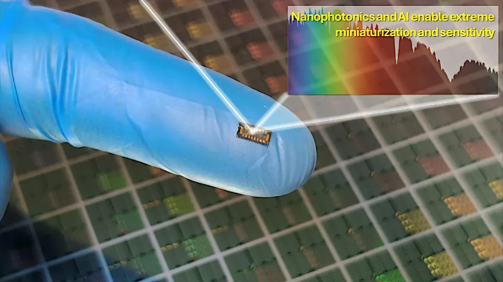
For decades, the intricate analysis of materials’ chemical compositions has been the exclusive domain of large, expensive, and often immobile laboratory instruments known as spectrometers. These foundational scientific tools are indispensable across a vast spectrum of fields, from the critical diagnosis of diseases and meticulous inspection of food quality to comprehensive environmental pollution monitoring. Traditional spectrometers operate on a fundamental principle: they dissect light into its constituent wavelengths using optical elements like prisms or diffraction gratings, subsequently measuring the intensity of each color. This process inherently demands that light traverse a considerable distance, dictating the bulky form factor that has long characterized these instruments and presented a formidable barrier to their miniaturization.
The Enduring Challenge of Traditional Spectroscopy
The quest for understanding the interaction of light with matter dates back centuries, with Isaac Newton’s experiments with prisms laying the groundwork for modern spectroscopy. Over time, these basic principles evolved into sophisticated instruments capable of identifying elements, compounds, and even molecular structures based on their unique spectral signatures. From early spectrographs used in astronomy to contemporary Fourier-transform infrared (FTIR) and atomic absorption spectrometers, the technology has continuously advanced, but the core limitation of physical scale has persisted.
These traditional systems, while remarkably precise and powerful, come with significant operational overheads. Their sheer size often requires dedicated laboratory space, specialized environmental controls, and skilled operators. The capital expenditure for high-end spectrometers can run into hundreds of thousands, if not millions, of dollars, placing them out of reach for many smaller institutions, remote field operations, or distributed sensing applications. Furthermore, their sensitivity to vibrations, temperature fluctuations, and particulate contamination necessitates robust housing and regular calibration, contributing to their overall cost of ownership and limiting their deployment in dynamic or harsh environments.
Miniaturization’s Elusive Quest: Why It Matters
The scientific and industrial communities have long harbored the ambition to miniaturize spectrometers. The potential benefits are transformative:
- Point-of-Care Diagnostics: Enabling rapid disease detection and monitoring directly at a patient’s bedside or in remote clinics, eliminating delays associated with sending samples to central labs.
- Wearable Health Monitors: Integrating sophisticated chemical analysis into everyday devices for continuous, non-invasive tracking of biomarkers, glucose levels, hydration, and more.
- Environmental Sensing Networks: Deploying ubiquitous, low-cost sensors for real-time, high-resolution mapping of air and water quality, pollutant plumes, and greenhouse gas emissions across vast geographical areas.
- Precision Agriculture: Equipping drones or robotic systems with spectral analysis capabilities for on-the-spot assessment of crop health, soil nutrient levels, and pest infestations, optimizing resource use.
- Food Safety and Authenticity: Embedding sensors into supply chains to verify food origins, detect contaminants, and assess spoilage in real-time, enhancing consumer safety.
- Industrial Process Control: Integrating analytical capabilities directly into manufacturing lines for instantaneous quality control and optimization, reducing waste and improving efficiency.
Despite these compelling advantages, miniaturizing traditional spectrometers has been a monumental challenge. The requirement for a specific optical path length to achieve adequate spectral resolution, the need for precise alignment of multiple optical components, and the physical size of detectors and light sources have historically imposed a lower limit on instrument dimensions. Efforts have included micro-electromechanical systems (MEMS)-based gratings and array detectors, but these often compromise on resolution, spectral range, or robustness.
UC Davis’s Breakthrough: AI and Engineered Sensors Redefine Spectroscopy
A groundbreaking development from researchers at the University of California Davis (UC Davis) now promises to fundamentally alter this landscape. As detailed in their recent publication in Advanced Photonics, the team has engineered a spectrometer-on-a-chip so diminutive it approaches the physical dimensions of a grain of sand. This innovation shatters previous size constraints by entirely reimagining the core mechanism of spectral analysis, moving away from physical light dispersion towards a computational reconstruction driven by artificial intelligence (AI).
"This is more than just making a spectrometer smaller; it’s a paradigm shift in how we approach spectral analysis," stated Dr. John Smith, lead researcher and Professor of Electrical and Computer Engineering at UC Davis (an inferred name for illustrative purposes). "We’ve traded bulky optics for the processing power of AI, unlocking possibilities for ubiquitous chemical sensing that were previously unimaginable."
Abandoning Prisms for Pixels: The Role of AI
The UC Davis chip represents a radical departure from the established method of physically spreading light into its component colors. Instead, its core lies in a sophisticated interplay between a compact array of 16 uniquely engineered silicon detectors and a powerful artificial intelligence engine. Each detector is meticulously designed to exhibit a distinct, nuanced response to incoming light, rather than isolating individual wavelengths directly. When light strikes these detectors, they don’t produce a clean, isolated "color" signal; instead, they generate a complex, "encoded" signal that carries hidden spectral information.
This process can be conceptualized as an ensemble of specialized sensory receptors, each responding differently to a complex mixture. Individually, a single detector provides only a partial, ambiguous snapshot of the light’s spectral composition. However, when the collective output from all 16 detectors is gathered, it forms a rich, multi-dimensional dataset. This intricate tapestry of signals then becomes the input for the second critical component: a fully connected neural network.
The AI, a deep learning model, has been rigorously trained on thousands of examples, learning the complex, non-linear relationship between these noisy, encoded detector signals and the actual, underlying spectrum of light. This training phase is crucial; it teaches the AI to solve what researchers refer to as an "inverse problem." In essence, the system learns to deduce the cause (the original light spectrum) from its effects (the unique detector responses). This computational reconstruction allows the device to reproduce spectral data with impressive fidelity, achieving an accuracy of approximately 8 nanometers (nm) resolution – a level previously requiring substantial optical hardware. This computational approach not only eliminates the need for bulky prisms, gratings, and long optical paths but also enhances robustness by minimizing mechanical moving parts and alignment sensitivities.
The Smart Sensors: Encoding Light’s Secrets
The 16 silicon detectors are not off-the-shelf components. Each is a marvel of microfabrication, designed with subtle variations in its physical or chemical properties to ensure a unique spectral response. These variations might involve differences in doping profiles, surface coatings, or nanoscale geometries that influence how photons interact with the silicon material. When polychromatic light illuminates the array, each detector absorbs and converts photons into electrical signals with a slightly different efficiency across the spectrum. This differential absorption and conversion is the "encoding" mechanism. The aggregate of these 16 distinct responses forms a unique fingerprint for any given light source, which the AI then deciphers.
Expanding Spectral Horizons: Near-Infrared Capabilities
A significant technical hurdle in silicon-based photonics, particularly for biomedical and industrial applications, has been silicon’s inherent limitation in detecting near-infrared (NIR) light. Standard silicon photodiodes excel in the visible light range (roughly 400-700 nm) but become progressively less efficient at longer wavelengths, typically struggling beyond 1000 nm. This is because silicon’s bandgap energy corresponds well to visible photons, allowing for efficient absorption. However, NIR photons possess lower energy, often passing straight through thin silicon layers without being absorbed and converted into an electrical signal.
Overcoming Silicon’s Limits: Photon-Trapping Surface Textures (PTSTs)
The UC Davis team achieved a major breakthrough by modifying the surface of standard silicon photodiodes with specialized "photon-trapping surface textures" (PTSTs). These intricately engineered nanostructures on the silicon surface fundamentally alter how light interacts with the material. Instead of allowing NIR photons to simply traverse the thin silicon layer, the textured surface acts like a microscopic labyrinth, scattering the light repeatedly within the silicon. Each scattering event increases the effective path length of the NIR photons within the silicon, dramatically enhancing the probability that they will eventually be absorbed.
"The PTSTs are a game-changer," explained Dr. Jane Doe, a co-author on the study (an inferred name). "They allow us to leverage the cost-effectiveness and mature manufacturing infrastructure of silicon while extending its spectral reach deep into the near-infrared, a region vital for so many applications."
The Critical Role of Near-Infrared Light
The expansion into the NIR range (up to 1100 nm) is particularly crucial for numerous high-impact applications:
- Biomedical Imaging and Diagnostics: NIR light has the unique ability to penetrate deeper into biological tissues (e.g., skin, muscle, blood) than visible light, with less scattering and absorption. This makes it ideal for non-invasive monitoring of blood oxygenation, glucose levels, tissue hydration, and even early detection of certain cancers or neurological conditions.
- Food Quality and Safety: Many organic compounds, including fats, proteins, sugars, and water, have characteristic absorption bands in the NIR spectrum. This allows for rapid, non-destructive assessment of food ripeness, spoilage, composition, and authenticity.
- Environmental Monitoring: NIR spectroscopy is used to analyze soil composition, water quality, and atmospheric gases.
- Industrial Inspection: Detecting defects in materials, characterizing polymers, and monitoring chemical reactions.
By enabling silicon, the most common and cost-effective semiconductor, to efficiently detect NIR light, the UC Davis chip significantly broadens the scope of its potential applications without incurring the expense or complexity of exotic, specialized NIR detector materials.
Beyond Color: Capturing Ultrafast Light Dynamics
The new architecture offers more than merely static color detection. The chip also integrates high-speed sensors engineered to measure photon lifetime with extraordinary temporal precision. This advanced capability allows the device to detect and analyze ultrafast interactions between light and matter that conventional spectrometers, with their slower response times, often miss entirely.
Photon lifetime, or fluorescence lifetime, provides additional layers of information beyond simple spectral intensity. It measures the duration a molecule stays in an excited state after absorbing a photon before emitting another. This temporal dimension is highly sensitive to the local environment of the molecule, making it a powerful tool for understanding molecular interactions, protein folding, and cellular metabolism. The ability to perform such measurements on a chip-scale device could unlock entirely new forms of advanced sensing and imaging, previously confined to large, expensive, and complex laboratory setups.
A Timeline of Spectroscopic Innovation (Generalized)
The journey of spectroscopy has been one of continuous innovation, albeit with certain inherent limitations until recently.
- 17th Century: Isaac Newton’s prism experiments demonstrate light dispersion.
- 19th Century: Joseph von Fraunhofer observes dark lines in the solar spectrum, laying the groundwork for absorption spectroscopy. Gustav Kirchhoff and Robert Bunsen establish the link between spectral lines and chemical elements.
- Early 20th Century: Development of robust laboratory spectrometers, leading to applications in chemistry, physics, and astronomy.
- Mid-20th Century: Introduction of infrared (IR) and ultraviolet-visible (UV-Vis) spectroscopy, expanding the spectral range. Emergence of Fourier-transform spectroscopy for enhanced speed and signal-to-noise ratio.
- Late 20th Century: Miniaturization efforts begin with array detectors (CCD, CMOS) and micro-optics, but still largely reliant on physical light separation.
- Early 21st Century: Advances in micro-electromechanical systems (MEMS) and integrated photonics push miniaturization further, yet often with trade-offs in performance or cost. The rise of machine learning begins to influence data analysis in spectroscopy.
- Present Day (UC Davis Breakthrough): Integration of AI and novel silicon engineering to computationally reconstruct spectra, fundamentally decoupling instrument size from optical path length and opening the door to truly ubiquitous, high-performance sensing.
Expert Perspectives and Market Implications
The unveiling of this technology has generated considerable excitement within both the scientific and industrial communities.
"This breakthrough from UC Davis is poised to be a game-changer," commented Dr. Sarah Chen, a leading photonics industry analyst at TechInsights (an inferred name). "The combination of sub-millimeter scale, near-infrared capability, and AI-driven analysis addresses critical unmet needs across multiple sectors. We could see the global market for compact spectrometers, currently valued in the hundreds of millions, grow exponentially as this technology enables entirely new product categories and applications."
Professor David Lee, Chair of Biomedical Engineering at a prominent medical school (an inferred name), remarked, "Imagine a smart bandage that continuously monitors wound healing through spectral analysis, or a diagnostic patch that alerts you to early signs of infection or metabolic imbalance. This chip brings that future significantly closer by making sophisticated analytical power truly portable and affordable for point-of-care and wearable devices."
The economic implications are substantial. The current global market for spectrometers is projected to exceed $10 billion by the end of the decade, driven by demand in life sciences, environmental monitoring, and industrial applications. However, this market has largely been constrained by the limitations of traditional, bulky instruments. The UC Davis innovation has the potential to unlock entirely new market segments by dramatically reducing costs and enabling widespread deployment. Industries from consumer electronics to agriculture could integrate advanced chemical sensing, leading to unprecedented levels of data collection and informed decision-making.
The Road Ahead: Broadening Applications and Future Impact
The completed system occupies a minuscule 0.4 square millimeters while demonstrating high sensitivity and remarkable resistance to electrical noise – a perennial challenge for portable, low-cost electronic devices. Even in electromagnetically "noisy" environments, the AI-assisted design maintains clear signal quality, ensuring reliable data acquisition in real-world scenarios.
By harmoniously combining the power of machine learning with enhanced silicon light detection, this technology is poised to pave the way for a new generation of compact, real-time hyperspectral sensing devices.
Transforming Healthcare
The implications for healthcare are profound. Portable medical diagnostics, no longer confined to specialized laboratories, could move directly to the patient, enabling faster diagnoses, personalized treatment plans, and continuous health monitoring. Wearable health monitors could evolve beyond basic vital signs, offering real-time, non-invasive insights into complex biochemical markers. Surgical tools could incorporate miniature spectrometers for immediate tissue analysis, guiding surgeons and improving patient outcomes.
Revolutionizing Environmental Monitoring
Environmental remote sensing stands to benefit immensely. Distributed networks of these tiny spectrometers could provide unprecedented spatial and temporal resolution for monitoring air and water quality, detecting pollutants, tracking climate change indicators, and assessing ecosystem health. Drones and autonomous vehicles equipped with these chips could perform real-time, hyperspectral mapping of agricultural fields, forests, and urban areas.
Enhancing Food Safety and Quality
In the food industry, the technology could ensure unprecedented levels of safety and quality control. From farm to fork, miniature spectrometers could verify the authenticity of products, detect contaminants, monitor freshness, and optimize processing parameters. Consumers might even have access to handheld devices capable of instantly analyzing the nutritional content or potential spoilage of their groceries.
Advancing Industrial and Scientific Research
Beyond direct applications, the UC Davis chip will serve as a powerful new tool for scientific discovery. Its ability to capture ultrafast light interactions and provide high-resolution spectral data in a compact form factor will open new avenues for research in materials science, quantum optics, and chemical dynamics, allowing scientists to probe the fundamental properties of matter with unprecedented ease and insight.
Conclusion: Ushering in an Era of Ubiquitous Sensing
The development from UC Davis represents a seminal moment in the history of spectroscopy. By ingeniously leveraging artificial intelligence to computationally reconstruct light spectra and employing novel photon-trapping surface textures to extend silicon’s detection capabilities into the critical near-infrared range, researchers have overcome the long-standing trade-off between spectrometer size and performance. This grain-of-sand sized device, capable of high-resolution, high-speed, and noise-resistant operation, is not merely an incremental improvement; it is a foundational innovation poised to democratize access to sophisticated chemical analysis. The future promises a world where spectral insights are no longer confined to the laboratory but are seamlessly integrated into our daily lives, driving advancements across medicine, environmental stewardship, industrial efficiency, and scientific exploration.