When the iconic Empire State Building ascended into the New York City skyline, its 102 stories were meticulously erected, piece by individual piece. For four decades, this feat of engineering stood as the world’s tallest structure, a testament to human ingenuity and construction. Decades later, uptown at Columbia University, Professor Oleg Gang and his chemical engineering laboratory are engaged in a different kind of monumental construction. While not building skyscrapers of steel and stone, their landmarks are infinitesimally small devices, meticulously crafted from nanoscopic building blocks that possess the remarkable ability to arrange themselves. This groundbreaking research, detailed in recent publications, heralds a new era in nanoscale manufacturing, offering unprecedented control and efficiency in creating complex three-dimensional structures.
A New Paradigm in Nanoscale Architecture
Professor Gang, a leading figure in chemical engineering and applied physics and materials science at Columbia Engineering, also heads the Soft and Bio Nanomaterials Group at Brookhaven National Laboratory’s Center for Functional Nanomaterials. He likens his lab’s achievements to a nanoscale rendition of the Empire State Building: "We can build now the complexly prescribed 3D organizations from self-assembled nanocomponents, a kind of nanoscale version of the Empire State Building." This remarkable capability is not merely an academic curiosity; it is poised to unlock advancements across a wide spectrum of critical technological fields.
"The capabilities to manufacture 3D nanoscale materials by design are critical for many emerging applications," Gang elaborated, "ranging from light manipulation to neuromorphic computing, and from catalytic materials to biomolecular scaffolds and reactors." The implications are far-reaching, promising to accelerate innovation in areas that demand precise control over matter at its most fundamental level.
The Dual Pillars of Innovation: Nature Materials and ACS Nano
The foundation for this transformative technology has been laid out in two seminal scientific papers. The first, published on July 9 in the prestigious journal Nature Materials, and the second, released on April 11 in ACS Nano, describe a novel methodology for fabricating targeted three-dimensional nanoscale structures through self-assembly. Crucially, the research also provides a detailed design algorithm, empowering other scientists and engineers to replicate and build upon these advancements.
At the heart of this revolutionary approach lies one of nature’s most fundamental molecules: DNA. This ubiquitous biological blueprint, known for its predictable folding patterns and ability to carry vast amounts of information, has been ingeniously repurposed as the primary building material for constructing intricate nanoscale architectures.
Moving Beyond Conventional Fabrication: The Limitations of Top-Down Approaches
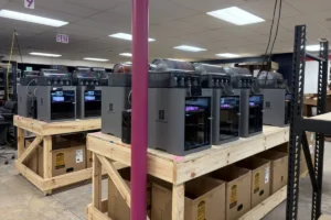
Historically, the fabrication of microelectronics and other small-scale devices has relied on "top-down" strategies. Techniques like photolithography, which employs light and intricate stencils to etch circuits onto materials, have been the workhorses of the industry. However, these methods face significant hurdles when it comes to creating complex, three-dimensional structures. Similarly, while additive manufacturing, commonly known as 3D printing, has made impressive strides, its resolution is still limited, making it incapable of fabricating features at the true nanoscale.
A fundamental inefficiency inherent in both photolithography and conventional 3D printing lies in their serial nature. Each feature is manufactured one by one, a process that, while effective for simpler designs, becomes exceptionally slow and resource-intensive when constructing complex three-dimensional objects. This limitation has been a persistent bottleneck in the development of next-generation nanoscale devices.
The Bottom-Up Revolution: Harnessing the Power of Self-Assembly
Professor Gang’s approach diverts from these conventional methods, drawing inspiration from the elegant efficiency of biological systems. His lab employs a "bottom-up" strategy, where nanoscale materials and devices are meticulously constructed through self-assembly processes, all guided by the precise instructions encoded within DNA. This method involves designing DNA strands that, under specific conditions, will fold and connect with other DNA components and embedded nanoparticles to form desired structures.
This methodology has been under continuous refinement through collaborative efforts with scientists across various disciplines. For instance, the team recently delivered a prototype to researchers at the University of Minnesota who are focused on developing 3D light sensors integrated directly onto microchips. The prototype was constructed by growing DNA scaffolds on a microchip and subsequently coating them with light-sensitive materials, demonstrating the practical application of Gang’s self-assembly techniques. This development, occurring approximately two months prior to the Nature Materials publication, showcases the rapid progress and tangible outcomes of the lab’s research.
Unveiling the "DNA Origami" Platform: Diverse Applications Emerge
The Nature Materials paper further solidifies the versatility of Gang’s approach, introducing an "inverse design strategy." This sophisticated method allows researchers to specify a desired three-dimensional nanoscale structure and then work backward to design the necessary DNA components and nanoparticles required for its self-assembly. The study highlights four compelling applications of this "DNA origami" approach:
- A Crystal-Like Structure: This design resulted in a meticulously ordered structure composed of one-dimensional strings and two-dimensional layers, mimicking the architecture of certain advanced materials.
- Solar Panel Mimic: The team successfully engineered a structure that replicates the material composition and functional properties found in common solar panels, paving the way for more efficient photovoltaic devices.
- Helical Crystal: Another innovative crystal structure was created, exhibiting a mesmerizing helical swirl, a form that could have applications in advanced optics or material science.
- Light-Reflecting Structures: For collaborator Nanfang Yu, a professor of applied physics at Columbia Engineering, the team designed a structure with specific light-reflecting properties. This research is a crucial step toward Yu’s long-term goal of creating an optical computer, a paradigm shift in computational technology.
Verifying Precision: Advanced Characterization and Parallel Fabrication
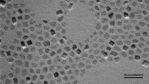
The accuracy and fidelity of these self-assembled structures were rigorously confirmed using cutting-edge characterization techniques. Advanced methods, including synchrotron-based X-ray scattering and electron microscopy, employed at both Columbia and Brookhaven National Laboratories, provided detailed insights into the assembled forms. These analyses not only verified that the resulting structures precisely matched the intended designs but also revealed key considerations for further improving structural integrity and precision.
Remarkably, each of these intricate structures assembled themselves spontaneously in simple water wells within Gang’s laboratory. This parallel fabrication process, where numerous components come together simultaneously during assembly, offers substantial advantages in terms of time and cost savings compared to the serial, one-by-one methods of traditional manufacturing. Furthermore, the entire process occurs in water, making it an environmentally friendly approach to creating advanced materials.
"This is a platform that is applicable to many materials with many different properties: biological, optical, electrical, magnetic," Professor Gang emphasized. "The end result simply depends on the design." This statement underscores the immense flexibility and broad applicability of the DNA-driven self-assembly platform.
Decoding the Blueprint: An Algorithm for Nanoscale Design
The challenge in designing complex nanoscale structures lies in translating a desired macroscopic form into the precise sequences of DNA building blocks required for self-assembly. DNA’s predictable pairing rules (adenine with thymine, and guanine with cytosine) are well-understood, but orchestrating the assembly of millions, if not billions, of individual components into a specific three-dimensional arrangement demands a sophisticated design strategy.
Gang and his colleagues have addressed this by developing an "inverse structural design" approach. "If we know the big structure with the function that we want to create, we can dissect that into smaller components to create our building blocks with structural, binding, and functional attributes required to form the desired structure," explained Professor Gang.
The fundamental building blocks are DNA strands engineered to fold into robust, eight-sided octahedral shapes, which Gang refers to as "voxels." These voxels feature connectors at each corner, enabling them to link together. By carefully designing the DNA sequences, numerous voxels can be programmed to connect in specific, repeating three-dimensional motifs, akin to how jigsaw puzzle pieces interlock to form a complex image. These repeating motifs then assemble in parallel to construct the final, hierarchically organized target structure.
MOSES: The Nano-Scale CAD Software
To facilitate this inverse design process, the researchers developed an algorithm to efficiently determine the minimal set of DNA voxels needed to create a desired structure. This algorithm, named Mapping Of Structurally Encoded aSsembly, or MOSES, functions like a nano-scale Computer-Aided Design (CAD) software. "You can think of it like compressing a file," said Jason Kahn, the first author of the Nature Materials paper and a staff scientist at BNL who was previously a postdoctoral researcher in Gang’s group. "We want to minimize the amount of information for the DNA self-assembly to be most efficient." MOSES provides the precise DNA voxel design required to assemble any arbitrarily defined three-dimensional lattice.
Adding Functionality: Nano-Cargo and Mineralization
Once the DNA scaffolding is assembled, it can be functionalized by incorporating various types of "nano-cargo" within the voxels. This nano-cargo imbues the final structure with specific properties. For instance, the inclusion of gold nanoparticles, as demonstrated in Professor Yu’s experiments, imparts unique optical characteristics. The research has shown that both inorganic and bio-derived nanocomponents can be seamlessly integrated into these DNA scaffolds.
Following the self-assembly of the device, the team can further enhance its durability through a process called "mineralization." This involves coating the DNA scaffolds with silica and then exposing them to heat. The heat decomposes the DNA, effectively converting the original organic scaffolding into a highly robust inorganic structure. This mineralization process ensures the longevity and stability of the nanoscale devices for practical applications.
The Road Ahead: Mimicking the Brain and Beyond
Professor Gang’s vision extends beyond current achievements. He continues to collaborate with Professor Sanat Kumar, a renowned chemical engineering professor at Columbia, and Professor Nanfang Yu, to uncover fundamental design principles that will enable the engineering of even more complex structures. A significant long-term goal is the creation of a three-dimensional circuit designed to mimic the intricate connectivity of the human brain, a feat that could revolutionize artificial intelligence and neuromorphic computing.
"We are well on our way to establishing a bottom-up 3D nanomanufacturing platform," Professor Gang stated with conviction. "We see this as a ‘next-generation 3D printing’ at the nanoscale, but now the power of DNA-based self-assembly allows us to establish massively parallel fabrication." This ambitious outlook suggests that the era of precise, efficient, and scalable nanoscale manufacturing is not a distant future, but a rapidly unfolding reality. The principles and technologies developed in Gang’s lab are poised to redefine what is possible in fields ranging from medicine and materials science to electronics and beyond, building a future one precisely assembled nanometer at a time.