For decades, ultrafast lasers have stood as formidable instruments in modern optics, their pulses, lasting mere hundreds of femtoseconds—or quadrillionths of a second—have enabled a spectrum of transformative technologies. From the meticulous demands of precision manufacturing and intricate eye surgery to the groundbreaking innovation of optical frequency combs, which earned a Nobel Prize and underpin the world’s most accurate optical atomic clocks, their influence is undeniable. Yet, despite their profound importance and widespread applications, these highly specialized lasers have largely remained substantial, capital-intensive systems, often consuming entire optical tables within research laboratories and industrial facilities. This physical footprint and associated costs have long presented a significant barrier to their broader adoption and integration into more compact, portable, or widely accessible devices.
A Paradigm Shift in Laser Technology
This long-standing challenge is now being addressed by a groundbreaking development from researchers at EPFL, led by Professor Tobias J. Kippenberg. Their recent work, published in the esteemed journal Nature, details a breakthrough that promises to dramatically reduce the size and cost of this critical technology. The team has successfully developed the first integrated ultrafast laser capable of matching the performance metrics traditionally associated with large, tabletop femtosecond laser systems. This pioneering device delivers impressive pulse energies of 1.05 nanojoules and achieves pulse durations as short as 147 femtoseconds, all while operating from a compact photonic chip. This achievement marks a significant leap forward, moving ultrafast laser technology from the realm of specialized laboratory equipment to the potential of mass-producible, chip-scale devices.
The Evolution of Ultrafast Lasers: A Brief Chronology
The journey of ultrafast lasers began in the 1960s with the invention of the mode-locked laser, which allowed for the generation of picosecond pulses. Subsequent decades saw continuous advancements, pushing pulse durations into the femtosecond regime.
- 1960s: First mode-locked lasers developed, generating picosecond pulses.
- 1980s: Advances in titanium-sapphire lasers and chirped pulse amplification (CPA) revolutionized ultrafast laser technology, enabling higher peak powers and shorter pulse durations in the femtosecond range. This was a critical step for many industrial and medical applications.
- 1990s-2000s: Fiber lasers began to emerge as a more robust and compact alternative to bulk solid-state lasers, though still relatively large compared to chip-scale devices. The development of optical frequency combs, pioneered by John L. Hall and Theodor W. Hänsch (Nobel Prize in Physics 2005), further cemented the importance of ultrafast lasers for precision metrology and atomic clocks.
- Present Day: Despite these evolutions, the fundamental challenge of miniaturization—especially for high-performance, high-pulse-energy systems—persisted. Traditional femtosecond lasers, whether solid-state or fiber-based, typically require intricate optical alignments, temperature control, and substantial power supplies, contributing to their large size (often spanning several square meters of an optical table) and high costs (ranging from tens of thousands to well over a million dollars, depending on specifications). This has limited their deployment to specialized laboratories, industrial settings with ample space, and high-budget research institutions.
The Promise and Challenge of Photonic Chips
Photonic chips represent a revolutionary approach to manipulating light. Analogous to how electronic chips process electrical signals, photonic chips guide and process light using microscopic structures known as waveguides, which are meticulously etched into a silicon or other semiconductor wafer. This technology has already proven transformative in various fields, most notably in telecommunications, where it has played a pivotal role in miniaturizing optical components and enabling high-speed data transmission over vast distances. The transition from bulky fiber optic components to integrated photonic circuits has led to smaller, more energy-efficient, and more reliable communication networks.
However, integrating ultrafast lasers onto these chips has presented a unique set of formidable challenges. The core difficulty lies in generating and maintaining high-energy, extremely short pulses within the highly confined environment of a chip. In such small waveguides, light interacts strongly with itself, leading to pronounced nonlinear optical effects. While these effects are crucial for pulse generation and shaping in ultrafast lasers, they can also easily destabilize the laser pulses, making it exceptionally difficult to achieve the desired performance metrics in a stable, integrated system. The delicate balance required between nonlinearity, dispersion management, and gain within a tiny footprint had long seemed insurmountable, leading many in the integrated photonics community to regard a high-pulse-energy femtosecond laser on a chip as a "holy grail" – an ultimate, yet elusive, goal.
Professor Kippenberg articulates this sentiment: "For more than twenty years, a high-pulse-energy femtosecond laser on chip was widely regarded as a holy grail of integrated photonics. Our result shows that it is not only possible, but that it can be achieved with a surprisingly elegant architecture that the integrated-photonics community had overlooked." This statement underscores the profound nature of the EPFL team’s achievement and the historical context of the challenge they have overcome.
An Elegant and Overlooked Design: The Mamyshev Oscillator
To achieve this remarkable feat, the researchers diverged from conventional integrated laser designs and adopted a specific laser architecture known as the Mamyshev oscillator. This design, while known in the broader laser physics community, had received comparatively little attention within the specialized field of integrated photonics. Its brilliance, in this context, lies in its inherent suitability for the unique characteristics of chip-scale light manipulation.
The core of the Mamyshev oscillator system involves placing a highly nonlinear waveguide between two distinct optical filters. Each filter is engineered to transmit only a specific, different portion of the light spectrum. As an intense laser pulse propagates through the nonlinear waveguide, its spectral content broadens significantly into a wider range of colors – a phenomenon driven by the intense light-matter interaction within the confined waveguide. Crucially, only the sufficiently broadened, intense part of this pulse can successfully pass through both optical filters, allowing it to continue circulating and be amplified within the laser cavity. Weaker light, conversely, does not undergo sufficient spectral broadening; it is effectively blocked by the filters and thus removed from the circulating cycle. This self-cleaning mechanism ensures that only high-energy, stable pulses are sustained.
Zheru Qiu, a co-leading author of the paper, highlights the key advantages of this design: "This design is especially attractive because it does not require any component that is difficult to make on this erbium-doped silicon nitride chip." This statement is critical because the complexity of fabrication is often a major hurdle in integrated photonics. By utilizing readily manufacturable components and materials (erbium-doped silicon nitride being a robust and well-understood platform), the team has ensured the practicality and scalability of their design.
Furthermore, Qiu emphasizes another significant benefit: the Mamyshev oscillator’s inherent resilience to the very nonlinear effects that often destabilize other laser architectures in confined photonic chips. Because photonic chips force light into extremely small waveguides, the interaction between light and the waveguide material, and indeed light with itself, is greatly amplified. While these nonlinearities are essential for pulse shaping, they can become unmanageable. The Mamyshev oscillator, however, is far less susceptible to these detrimental problems, making it an ideal candidate for integrated photonic devices where nonlinear interactions are both prevalent and intense. This design choice was not merely an innovation but a strategic selection that perfectly leveraged the unique environment of a photonic chip.
Miniaturization and Manufacturing: Unlocking Unprecedented Accessibility
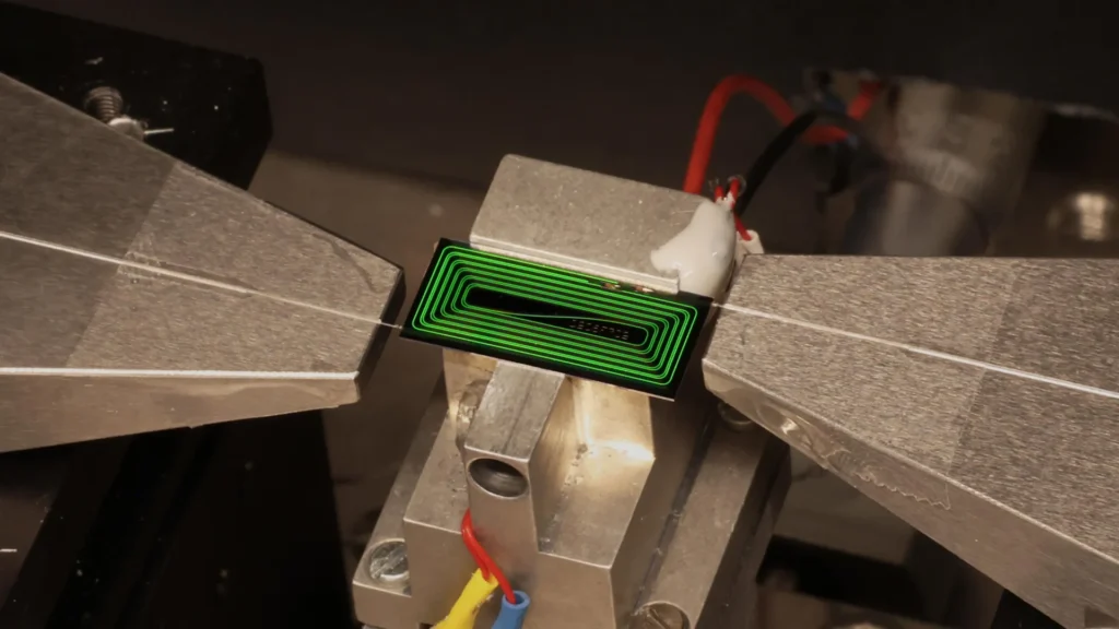
The physical dimensions of this integrated laser are truly astounding when compared to its traditional counterparts. The laser cavity itself measures 42 centimeters in length, yet through clever engineering and compact folding, it is integrated onto a chip occupying roughly the area of a match head. To put this into perspective, conventional fiber-based ultrafast lasers, while more compact than bulk solid-state systems, still typically require footprints of several square feet and intricate packaging. The EPFL device represents a reduction in volume by several orders of magnitude, moving from desktop-sized instruments to a mere speck on a chip.
This dramatic miniaturization is coupled with an equally significant manufacturing advantage. Photonic chips can be produced at wafer scale, employing fabrication methods highly analogous to those used for the mass production of computer chips. This means that, in principle, thousands of these laser cavities—potentially more than 1,000—could be produced simultaneously on a single wafer. Such an economy of scale is poised to fundamentally transform the cost landscape of ultrafast lasers. Currently, even entry-level femtosecond lasers can cost tens of thousands of dollars, with high-performance systems easily exceeding half a million. Wafer-scale manufacturing could reduce the per-unit cost by orders of magnitude, democratizing access to this powerful technology.
This manufacturing paradigm shift would not only make ultrafast lasers more affordable but also significantly expand their availability. Industries and research fields that previously found the cost and size prohibitive could now integrate these lasers into their operations. This could foster innovation across numerous sectors, from advanced material processing to environmental monitoring and medical diagnostics.
Broadening the Horizon: Applications and Future Impact
The implications of this breakthrough are far-reaching, promising to extend the utility of ultrafast lasers into novel applications and make existing ones more efficient and accessible.
- Precision Manufacturing: Ultrafast lasers are indispensable for micro-machining, drilling, and cutting with extreme precision, minimizing heat-affected zones. With chip-scale lasers, manufacturing processes could be localized, integrated into smaller production lines, or even deployed in distributed manufacturing models. This could lead to more compact, versatile tools for producing components for electronics, medical devices, and aerospace.
- Medical Diagnostics and Surgery: In ophthalmology, femtosecond lasers are standard for LASIK eye surgery, offering unparalleled precision. Miniaturized versions could enable more portable surgical tools, expand access to advanced eye care in remote areas, and pave the way for new in-vivo imaging techniques, such as deeper tissue imaging with higher resolution and less invasiveness. The ability to perform medical diagnostics at the point of care, for example, identifying disease biomarkers or analyzing tissue samples with high accuracy, becomes a tangible reality.
- Environmental Sensing and Spectroscopy: The exquisite spectral breadth of ultrafast lasers makes them ideal for spectroscopy, allowing for the precise identification and quantification of various substances. Chip-based lasers could lead to portable, handheld devices for detecting environmental pollutants in air and water, monitoring industrial emissions, or even analyzing agricultural soil composition in the field. This would move sophisticated analytical capabilities out of specialized laboratories and into everyday use.
- Material Science and Non-Destructive Testing: Ultrafast lasers are used to probe the fundamental properties of materials and identify hidden defects without causing damage. Compact versions could be integrated into automated inspection systems for quality control in manufacturing, allowing for rapid and thorough analysis of materials like composites, semiconductors, and advanced alloys.
- Optical Atomic Clocks and Navigation: Optical frequency combs, derived from ultrafast lasers, are the heart of the world’s most accurate atomic clocks, crucial for global navigation satellite systems (GNSS) like GPS, high-speed telecommunications, and fundamental physics research. Miniaturizing the laser component is a critical step towards creating compact, portable optical atomic clocks. These could dramatically enhance the precision of navigation systems, enable more secure data transmission, and facilitate deep-space communication with unprecedented accuracy. Imagine personal devices or autonomous vehicles equipped with atomic clock-level precision, impervious to traditional jamming.
- Quantum Technologies: Ultrafast lasers are increasingly vital in quantum computing and quantum sensing, providing the precise control and manipulation of quantum states. Chip-scale, high-performance ultrafast lasers could accelerate the development of practical quantum devices, reducing their footprint and operational complexity.
According to Qiu, "With kilowatt-level peak powers, the chip can drive demanding applications that have long depended on large, expensive laboratory lasers." This statement underlines the critical performance capabilities of the integrated device, demonstrating that miniaturization does not come at the expense of power or utility. The peak power generated by these femtosecond pulses is sufficient for inducing nonlinear optical phenomena necessary for many advanced applications.
The researchers envision a future where this technology leads to widely available, portable, and affordable devices that can perform sophisticated tasks, such as detecting environmental pollutants in real-time, identifying hidden defects in materials during production, and performing rapid, accurate medical diagnostics in clinics or even homes. Furthermore, the development could significantly contribute to the creation of compact, robust optical atomic clocks, which are expected to play increasingly important roles in future communications networks, advanced navigation systems, and even in defining new standards for time and frequency.
The collaborative effort behind this pioneering work involved researchers from the EPFL Institute of Electrical and Microengineering and the Helmholtz-Zentrum Dresden-Rossendorf (HZDR), highlighting the interdisciplinary nature of modern scientific breakthroughs. As this technology matures, the next steps will likely involve further integration of other optical components onto the chip, scaling up power for even more demanding industrial applications, and ultimately, moving towards commercialization to bring these revolutionary devices to a wider global market. The long-sought "holy grail" of integrated photonics has not only been found but has opened a new frontier for precision technology.