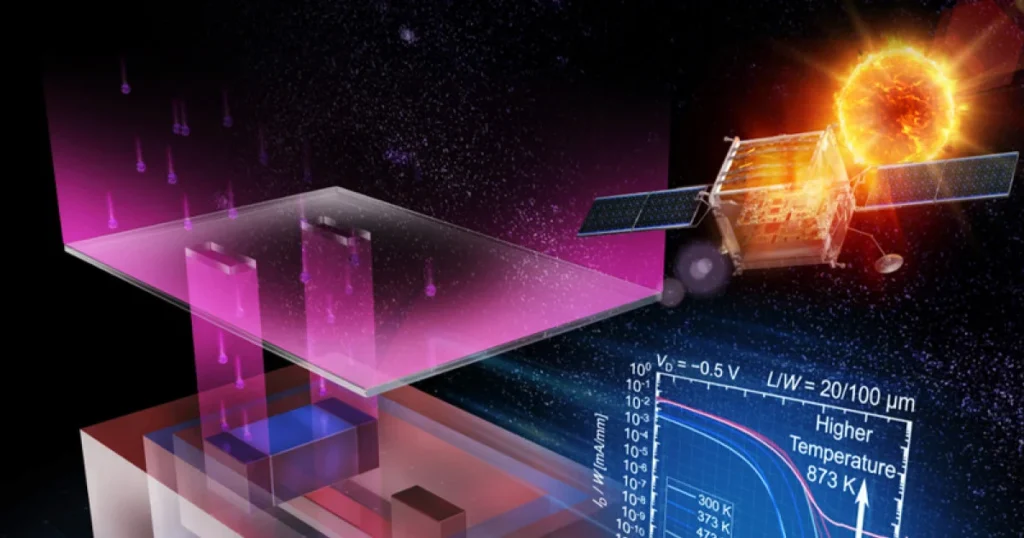
Engineers and scientists are continually pushing the boundaries of material science and semiconductor technology, seeking devices that can withstand increasingly demanding operational parameters. In a significant advancement, a team of researchers from Kyoto University has demonstrated a novel silicon carbide (SiC) junction field-effect transistor (JFET) capable of stable operation at unprecedented temperatures of up to 600°C. This breakthrough is particularly notable because it leverages standard ion implantation techniques, a common process in modern semiconductor manufacturing, suggesting a more direct path to commercial viability for extreme-temperature electronics.
The Technical Breakthrough: Operating at 600°C
The core of this innovation lies in the meticulous design and fabrication of the SiC JFET. Silicon carbide, a wide-bandgap semiconductor, has long been recognized for its superior properties compared to conventional silicon, particularly its ability to withstand higher voltages, operate at elevated temperatures, and conduct heat more efficiently. These characteristics have already made SiC a material of choice for power electronics, such as in electric vehicles and renewable energy systems, where efficiency and robustness under stress are paramount. However, extending SiC’s capabilities to reliable logic circuits operating at truly extreme temperatures, like 600°C, presents a much more complex set of engineering challenges.
Understanding Silicon Carbide
To appreciate the significance of 600°C operation, it’s crucial to understand the inherent advantages of SiC. Silicon, the workhorse of the semiconductor industry, typically begins to suffer performance degradation and reliability issues above 200°C. Its bandgap, the energy required to free an electron from its bound state, is relatively narrow (1.12 eV). SiC, in contrast, boasts a much wider bandgap (approximately 3.2 eV for 4H-SiC, a common polytype), meaning more energy is required to excite electrons into the conduction band. This wider bandgap translates directly into several key benefits: higher breakdown voltage, lower leakage currents at elevated temperatures, and superior thermal conductivity, allowing devices to dissipate heat more effectively. These properties make SiC an ideal candidate for pushing the thermal limits of electronics.
Overcoming Manufacturing Hurdles: Ion Implantation and Dopant Channeling
One of the primary hurdles in fabricating high-performance SiC devices, especially at extreme temperatures, lies in the manufacturing process itself. The Kyoto University team was committed to utilizing processes already established within modern semiconductor fabrication facilities to accelerate adoption. Their chosen method, standard ion implantation, involves bombarding the semiconductor material with ions (dopants) to precisely alter its electrical conductivity. While widely used, ion implantation in SiC can suffer from a phenomenon known as dopant channeling, where implanted ions penetrate deeper into the material than intended, leading to unpredictable electrical characteristics and performance variations.
To counteract this, the researchers developed a novel bottom-gate structure. This design provides enhanced control over the electrical properties of the transistor, particularly the threshold voltage – the voltage required to switch the transistor on. By refining this structure, they achieved a remarkable improvement in predictability. At 400°C, the deviation between the designed and measured threshold voltage was drastically reduced from over 2 volts to less than 0.1 volts. This level of precision is critical for building complex, reliable integrated circuits, where consistent transistor behavior is essential.
Innovative Isolation: Tackling Substrate Leakage
Another significant challenge addressed by the Kyoto team was the issue of leakage current through the SiC substrate at high temperatures. While SiC provides excellent electrical isolation at ambient temperatures, its insulating properties degrade as temperatures climb. This degradation can lead to unwanted current paths, compromising the device’s performance and potentially causing failures. To mitigate this, the researchers introduced a double-well isolation structure. This design essentially encases each individual transistor within its own pn junction, effectively creating an electrical barrier that prevents stray currents from flowing through the substrate. The team reported that the residual leakage current in their design approached the theoretical limit imposed by the intrinsic properties of SiC itself, indicating an exceptionally effective isolation scheme.
A Shift Towards Standardized Fabrication
The Kyoto University team’s choice to employ standard ion implantation techniques represents a pivotal aspect of their breakthrough. Historically, previous efforts to develop extreme-temperature SiC electronics, including systems deployed by NASA that have successfully operated above 500°C, have often relied on specialized, often complex, and costly manufacturing processes. These bespoke techniques, while effective for specific high-performance applications, typically lack the scalability and cost-effectiveness required for widespread industrial adoption.
Economic and Scalability Implications
By demonstrating 600°C operation using standard fabrication methods, Kyoto University has opened the door to potentially integrating these advanced SiC devices into existing semiconductor manufacturing lines with fewer modifications. This has profound economic and scalability implications. Standardized processes can significantly reduce manufacturing costs, accelerate production cycles, and increase overall yields, making high-temperature SiC electronics more accessible and economically viable for a broader range of applications. It shifts the paradigm from niche, custom-built solutions to a more mainstream, industrial-scale approach, which is crucial for market penetration and widespread technological impact. Industry analysts project that the global SiC market, valued at approximately $2 billion in 2023, is poised for substantial growth, potentially reaching over $10 billion by 2032, driven largely by advancements in power electronics and, increasingly, by these emerging extreme-environment applications. This research aligns perfectly with the industry’s push for more robust and cost-effective SiC solutions.
Current Limitations and Future Development
Despite the remarkable achievement, the researchers acknowledge that there are still several limitations to address before these SiC transistors can be widely deployed. The current prototype is a "normally-on" device, meaning it conducts electricity even without an applied gate voltage. While functional, this characteristic leads to continuous standby power consumption, making it unsuitable for highly efficient complementary logic circuits, which are the bedrock of modern digital electronics. Complementary logic typically relies on both normally-on (n-type) and normally-off (p-type) transistors working in tandem to minimize power dissipation.

The "Normally-On" Challenge and Complementary Logic
The Kyoto team has previously demonstrated complementary SiC JFET logic at 350°C, and their next critical step involves developing "normally-off" devices using this new 600°C-capable structure. Achieving reliable normally-off operation at such extreme temperatures is essential for building complex, low-power digital circuits that can process information efficiently in harsh environments. This development would unlock the full potential for integrated systems, moving beyond simple sensing or power control to onboard data processing and intelligent control.
Beyond the Transistor: Packaging and Long-Term Reliability
Another significant challenge lies beyond the transistor itself: long-term reliability and packaging. While creating a transistor that can survive 600°C is a monumental achievement, an entire electronic system requires interconnects, passivation layers, packaging materials, and other peripheral components that can also endure the same extreme environment for extended periods. Conventional materials and packaging techniques designed for room temperature or moderate heat simply will not suffice. Developing robust, high-temperature-resistant wiring, substrates, and hermetic seals that prevent environmental degradation (e.g., oxidation, corrosion) at 600°C for thousands of hours is a substantial engineering challenge that requires collaborative efforts across material science, mechanical engineering, and electrical engineering disciplines. Without these advancements, the full potential of these extreme-temperature transistors cannot be realized.
Transformative Applications Across Industries
The ability of electronics to operate at 600°C without external cooling introduces engineers to application spaces that were previously considered inaccessible or required complex, bulky, and expensive thermal management systems. This breakthrough promises to revolutionize several critical sectors.
Aerospace and Defense: Unlocking New Frontiers
Gas turbines and jet engines are prime examples of systems that generate enormous amounts of heat during operation. Currently, sensors and control electronics in these systems must be located away from the hottest sections, often requiring long, shielded connections to cooler areas. High-temperature SiC electronics could enable sensors and processing units to be placed directly within the engine’s hot sections, providing more accurate, real-time data for performance monitoring, diagnostics, and control. This proximity could lead to significant improvements in engine efficiency, safety, and lifespan, while also reducing the weight and complexity associated with extensive cabling and cooling infrastructure. Furthermore, applications in hypersonic flight, re-entry vehicles, and advanced propulsion systems, where extreme aerodynamic heating is a major constraint, could greatly benefit from such robust electronics, enabling smarter, more resilient aerospace platforms.
Deep Space Exploration: Enduring Venus’s Inferno
Perhaps one of the most intriguing and challenging applications is the exploration of Venus. With a crushing atmospheric pressure 92 times that of Earth and surface temperatures averaging around 465°C, Venus’s environment is notoriously hostile to conventional electronics. Traditional silicon-based spacecraft components can only operate for minutes without substantial, heavy, and complex thermal protection systems, severely limiting mission duration and scientific data collection. A transistor capable of operating at 600°C could fundamentally change Venusian exploration, allowing future probes to perform sensing, data acquisition, and even processing directly within the Venusian atmosphere and on its surface for extended periods. This would enable unprecedented scientific insights into Venus’s geology, atmosphere, and potential habitability. Beyond Venus, such robust electronics could also find use in solar probes operating close to the sun or in probes exploring the hot interiors of gas giants’ moons, where radiation and temperature extremes are prevalent.
Industrial Processes and Energy Sector Efficiency
The same principle of close-proximity electronics applies to a wide array of industrial equipment operating at extreme temperatures. Furnaces, chemical reactors, glass manufacturing plants, and other high-temperature processing systems could utilize these SiC electronics to place sensors, actuators, and control modules directly within the hot zones. This direct placement would eliminate the need to isolate sensitive components from the heat, leading to more precise process control, improved safety, reduced energy consumption, and enhanced operational efficiency. In the energy sector, high-temperature SiC devices could revolutionize geothermal energy systems, allowing electronics to operate deep within boreholes where temperatures are extremely high, enabling more efficient energy extraction and monitoring. Similarly, nuclear facilities could benefit from sensors and control systems capable of withstanding intense heat and radiation, enhancing safety and operational capabilities.
Automotive and Electric Vehicles
While not explicitly mentioned in the original article, the automotive industry, particularly in the context of electric vehicles (EVs) and advanced internal combustion engines, stands to benefit significantly. SiC is already making inroads into EV power electronics due to its efficiency. Extending its application to high-temperature logic could enable more integrated control units closer to the engine or motor, reducing wiring harnesses, weight, and EMI susceptibility. For traditional internal combustion engines, placing sensors directly within the exhaust system or combustion chamber could lead to more accurate real-time diagnostics and better emission control.
The Broader Landscape of Wide-Bandgap Semiconductors
The Kyoto University research is not an isolated effort but part of a larger, global trend towards developing wide-bandgap (WBG) semiconductors like SiC and Gallium Nitride (GaN). These materials are at the forefront of enabling the next generation of power electronics, high-frequency communications, and extreme-environment systems. Governments and industries worldwide are investing heavily in WBG research and manufacturing due to their strategic importance for energy efficiency, defense, and space exploration. This context underscores the significance of Kyoto’s achievement, positioning it as a key step in advancing the capabilities of the entire WBG semiconductor ecosystem. The ability to produce such high-performance devices using standard processes is a critical enabler for accelerating the adoption of WBG technologies beyond niche high-end applications.
Conclusion: A Catalyst for Extreme Electronics
The development of a SiC JFET capable of 600°C operation using standard ion implantation techniques represents a pivotal moment in the quest for extreme-environment electronics. The meticulous design, incorporating a bottom-gate structure to combat dopant channeling and a double-well isolation scheme to mitigate substrate leakage, showcases sophisticated engineering. While challenges remain, particularly in developing normally-off devices for complementary logic and in addressing the complex issues of packaging and long-term reliability for entire systems, the foundation laid by Kyoto University is robust.
This breakthrough has the potential to unlock entirely new possibilities across aerospace, defense, deep space exploration, industrial automation, and energy sectors. By reducing reliance on bulky cooling systems and enabling electronics to operate directly within harsh conditions, this technology promises to foster more efficient, resilient, and intelligent systems. If researchers can successfully transition to normally-off versions and resolve the outstanding integration and reliability hurdles, silicon carbide could indeed become the material that allows electronics to thrive in environments where conventional silicon simply cannot survive, marking a new era for robust and pervasive electronic intelligence.