The escalating demand for computational power, driven by the rapid expansion of artificial intelligence, high-performance computing, and mobile technology, has brought the global semiconductor industry to a critical crossroads. As engineers strive to pack more transistors into increasingly smaller footprints, the primary obstacle to progress is no longer just the physical limit of transistor size, but the management of the immense heat these components generate. In a breakthrough study published in Nature Communications, a multidisciplinary team of researchers at the Massachusetts Institute of Technology (MIT) has demonstrated a novel diagnostic technique that uses ultrafast X-rays and laser pulses to visualize heat flow within multilayered electronic devices with unprecedented precision.
This new methodology addresses a long-standing "blind spot" in semiconductor manufacturing. While traditional thermal imaging tools can provide a general overview of a device’s surface temperature, they lack the depth and resolution required to see how heat moves through the internal, stacked layers that characterize modern chip architectures. By successfully mapping these internal thermal dynamics, the MIT team has revealed how microscopic defects—some as small as a single micron—can catastrophically impede heat dissipation, potentially leading to device failure or significant performance throttling.
The Thermal Wall: A Modern Computing Crisis
For decades, the semiconductor industry followed the trajectory of Moore’s Law, which predicted the doubling of transistors on a microchip approximately every two years. However, this miniaturization has led to the "thermal wall." As chips become more power-dense, they generate heat at levels that are increasingly difficult to dissipate. In high-stakes environments like data centers, which power everything from cloud storage to generative AI models, cooling systems now account for a staggering portion of total energy consumption. On a consumer level, this manifests as the overheating of laptops and smartphones, which often results in "thermal throttling," where the device intentionally slows its processor to prevent physical damage.
The difficulty in solving this problem lies in the complexity of modern electronic materials. Today’s devices are rarely made of a single material; instead, they are intricate "sandwiches" of various semiconductors, insulators, and conductors. Each interface between these layers represents a potential barrier to heat flow. Understanding how "heat carriers"—the atomic-level vibrations known as phonons—navigate these interfaces is essential for designing the next generation of efficient electronics.
Limitations of Traditional Thermal Metrology
Prior to the MIT breakthrough, researchers relied on several standard methods to measure thermal conductivity, each with significant drawbacks for multilayered systems. One common technique, known as Time-Domain Thermal Reflectance (TDTR), uses laser pulses to measure how the surface of a material changes its reflectivity as it cools. While highly accurate for bulk materials or single-layer films, TDTR is limited by the physics of light. Visible light cannot penetrate deep into a multilayered stack, meaning it provides an "average" signal of the entire device rather than specific data for buried layers.
Similarly, infrared (IR) thermography, while useful for macroscopic observations, lacks the spatial resolution to see what is happening at the nanometer or micrometer scale. IR cameras also suffer from slow frame rates, making it impossible to capture the "ultrafast" thermal events that occur when a transistor switches on and off in a fraction of a microsecond.
"Chip developers need devices that can handle heat," says Mingda Li, an associate professor of nuclear science and engineering at MIT and a co-corresponding author of the study. "I think overheating has become the real bottleneck in device performance. When doing these diagnoses using traditional techniques, they couldn’t get down to the micro- or nanometer scale. But eventually, they’d like to go beyond that to study the heat carriers and understand exactly what causes failure."
A Synergistic Approach: Combining X-Rays and Lasers
To overcome these barriers, the MIT researchers, in collaboration with scientists from the Argonne National Laboratory and the University of Texas at Austin, turned to a sophisticated combination of high-energy physics and ultrafast optics. The team utilized one of the brightest X-ray sources in the world at a national laboratory facility to probe the internal structure of their test devices.
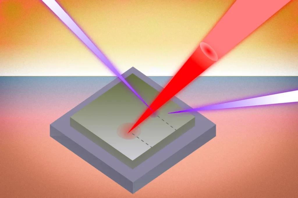
The technique works by using a laser pulse to deliver a precise "heat kick" to the material. Almost simultaneously, an ultrafast X-ray beam scans the device. Because X-rays have a much shorter wavelength than visible light, they can penetrate through multiple layers of a chip. As the heat moves through the material, it causes the atomic lattice to expand and vibrate, a phenomenon known as thermal strain. The X-rays detect these subtle changes in the lattice structure through diffraction patterns, allowing the researchers to "see" the heat as it propagates from one layer to the next in real-time.
This dual-probe approach—using lasers for excitation and X-rays for detection—allows for a level of depth-resolved sensing that was previously impossible. It enables engineers to distinguish between the heat moving through a top layer of gallium nitride and the heat crossing the interface into a bottom layer of silicon.
The Micro-Defect Discovery: A Fourfold Reduction in Efficiency
The researchers tested their method on a device composed of gallium nitride (GaN) on a silicon substrate. GaN is a "wide-bandgap" semiconductor that is highly prized in the industry for its ability to handle high voltages and conduct heat more efficiently than traditional silicon. It is increasingly used in 5G infrastructure, electric vehicle power converters, and fast-charging adapters.
However, the manufacturing process for GaN-on-silicon often introduces "wrinkles" or microscopic defects where the two materials meet. Using their new X-ray technique, the MIT team quantified the impact of a single micron-scale wrinkle defect. The results were startling: the defect caused a fourfold reduction in the material’s ability to transfer heat at that specific spot.
Furthermore, the team discovered that the defect introduced "thermal anisotropy"—meaning the heat did not spread out evenly in all directions. Instead, it moved more easily in one direction than another, creating unpredictable "hotspots." In a real-world processor, such a hotspot could cause a localized failure while the rest of the chip remains at a safe temperature, making the failure difficult to diagnose with traditional tools.
"When people model heat dissipation, they model perfect crystals without defects," explains Professor Li. "But these types of large wrinkle defects are very common in 2D materials. People never even knew how much heat is blocked by these wrinkles. Those are things we can now directly observe with this technique."
Industry Implications and Future Applications
The implications of this research extend far beyond academic curiosity. A leading semiconductor industry consortium has already expressed interest in collaborating with the MIT team to apply this measurement technique to commercial chip designs. As the industry moves toward "3D ICs" (integrated circuits), where layers of logic and memory are stacked on top of each other like a skyscraper, the ability to map heat in three dimensions becomes a prerequisite for reliability.
AI and Data Centers
In the realm of Artificial Intelligence, the hardware required to train large language models generates unprecedented thermal loads. If companies can use the MIT technique to identify exactly where heat is getting trapped in their GPU architectures, they can redesign those interfaces to be more "thermally transparent," leading to chips that can run at higher clock speeds without melting.
Clean Energy and EVs
For the clean energy sector, more efficient heat management in power electronics means less energy is wasted as heat during the conversion process in electric vehicles or solar inverters. This directly translates to longer range for EVs and higher efficiency for the power grid.
Wearable Technology
In wearables, where electronics are in direct contact with human skin, thermal management is a matter of safety and comfort. The MIT technique could allow for the development of more powerful sensors in smaller, flexible form factors that remain cool to the touch.
Analysis of the Research Chronology
The development of this technique represents the culmination of several years of advancement in X-ray science. The emergence of Free-Electron Lasers (XFELs) and high-brightness synchrotrons provided the necessary "probes" to see at the atomic scale.
- Initial Theory (Pre-2020): Researchers hypothesized that thermal strain could be mapped using X-ray diffraction, but the temporal resolution required to capture heat flow in semiconductors was lacking.
- Facility Upgrades: Facilities like the Advanced Photon Source at Argonne National Laboratory underwent upgrades that allowed for shorter, more intense X-ray pulses.
- MIT Integration: The MIT team developed the specific laser-heat-sync protocols and the mathematical models required to interpret the diffraction data as specific heat-flow measurements.
- Verification: The 2024 publication in Nature Communications serves as the definitive proof of concept, demonstrating that the technique works on realistic, multilayered semiconductor architectures.
Conclusion: Designing a Cooler Future
The MIT research represents a shift from reactive to proactive thermal management. Instead of building a chip and then trying to figure out how to cool it with external fans or liquid systems, engineers can now use this X-ray methodology to design chips that are inherently better at moving heat away from their own sensitive components.
"This will enable better thermal design of electronic systems," says co-corresponding author and MIT Associate Professor Jeehwan Kim. "Even with the same type of materials, the geometry and how the materials are laid out is quite complicated. This technique will show us how those differences impact thermal flow by providing direct experimental measurements. It is something the industry has been longing for."
As the world continues its transition into an era of ubiquitous computing and AI-driven infrastructure, the ability to see the "invisible" movement of heat through the heart of our machines may be the most important tool in ensuring that the digital revolution does not overheat. The work was supported by the U.S. Department of Energy, the U.S. National Science Foundation, and the MIT School of Engineering, signaling a broad institutional recognition of the importance of thermal science in the future of global technology.