In the intricate realm of quantum materials, where the rules of classical physics often bend, the emergence of electronic order is a phenomenon of profound scientific interest. Unlike the smooth, predictable behaviors seen in many macroscopic systems, electronic order at the quantum scale frequently manifests in complex, non-uniform patterns that fluctuate across different regions of a material. A quintessential example of this is the charge density wave (CDW), a fascinating state where electrons collectively organize into repeating, periodic patterns, typically at cryogenic temperatures. While CDWs have been a cornerstone of condensed matter physics research for decades, a persistent challenge has been the direct observation of how their strength, known as amplitude, and their spatial coherence – the extent to which these patterns connect across space – change during a phase transition, where a material shifts from one state to another. This knowledge gap has hindered a complete understanding of the fundamental mechanisms governing these exotic electronic states.
A significant breakthrough, poised to redefine our understanding of these quantum phenomena, has been achieved by a distinguished research team. Led by Professor Yongsoo Yang of the Department of Physics at the Korea Advanced Institute of Science and Technology (KAIST), and involving collaborations with Professors SungBin Lee, Heejun Yang, and Yeongkwan Kim from KAIST, alongside researchers from Stanford University, the team has successfully achieved the unprecedented: directly visualizing the spatial evolution of charge density wave order within a quantum material. This landmark achievement provides an invaluable, high-resolution window into the dynamic processes that dictate the formation, persistence, and eventual breakdown of electronic order.
The Enigma of Charge Density Waves: A Background
Quantum materials are a class of substances that exhibit unique electronic and magnetic properties arising from quantum mechanical effects. These materials hold immense promise for revolutionary technologies, from high-temperature superconductors to next-generation quantum computers. Understanding their fundamental properties is therefore paramount. Charge density waves are one such property, representing a collective state of electrons where their density becomes periodically modulated, forming a wave-like pattern across the crystal lattice. This phenomenon is analogous to ripples forming on a pond, but at an atomic scale, involving the collective behavior of countless electrons.
First theorized in the 1930s and experimentally confirmed in the 1970s, CDWs are found in various low-dimensional materials, including transition metal dichalcogenides and certain cuprates. Their presence can significantly influence a material’s electrical conductivity, optical properties, and even its potential for superconductivity. For instance, in some materials, the formation of a CDW competes with superconductivity, while in others, it might coexist or even facilitate it. Despite their recognized importance, the transient and spatially heterogeneous nature of CDWs has made them notoriously difficult to study with conventional methods. Traditional techniques like X-ray diffraction provide an average picture of the material’s structure, revealing the presence of CDW order but offering limited insight into its local variations or how it evolves dynamically. Scanning probe techniques, such as scanning tunneling microscopy (STM), offer high spatial resolution but are often limited to surface analysis and can struggle with probing the full temperature range of a phase transition while maintaining atomic precision. The challenge has always been to combine both high spatial resolution and the ability to track dynamic changes across a broad temperature spectrum, especially deep within the bulk of the material.
A New Window into Nanoscale Dynamics: The Technological Leap
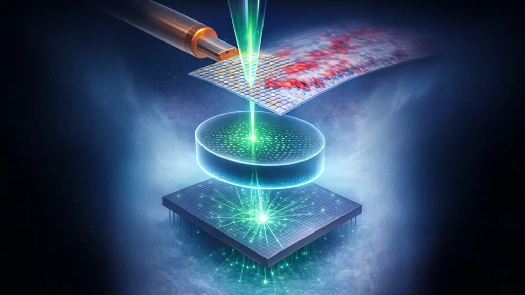
To overcome these long-standing observational hurdles, the KAIST-Stanford team employed an exquisitely advanced experimental setup: a liquid-helium-cooled electron microscope integrated with four-dimensional scanning transmission electron microscopy (4D-STEM). This sophisticated technological synergy was the cornerstone of their breakthrough.
The electron microscope, cooled to temperatures approaching absolute zero (near -253°C, or 20 Kelvin), is critical for stabilizing the delicate quantum states and minimizing thermal noise that would otherwise obscure the subtle electronic patterns. At such extreme cryogenic conditions, the material’s electrons can settle into their ordered CDW states, allowing for clear observation. The "four-dimensional" aspect of 4D-STEM refers to its ability to collect a full electron diffraction pattern at every point in a scanned area, effectively providing a wealth of information about local crystal structure, strain, and electronic order, not just a simple image. This advanced microscopy technique allowed the researchers to not only image structures with astonishing resolution—resolving features as small as one hundred-thousandth the width of a human hair—but also to track the intricate dance of CDW formation, weakening, and disintegration as the temperature was precisely varied.
Crucially, this setup enabled the creation of detailed nanoscale maps. These maps went far beyond merely indicating the presence of electronic order; they quantitatively depicted its strength (amplitude) and, for the first time, revealed how this order connects and propagates across different regions of the material (spatial coherence). This level of detail offers an unprecedented view, akin to watching a time-lapse video of ice crystals forming on a lake, but at a resolution millions of times finer and with direct insight into the underlying electronic structure.
Unveiling the Patchwork: Key Observations and Findings
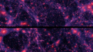
The high-resolution imaging brought forth several groundbreaking observations that challenge conventional assumptions about electronic order. The most striking finding was that electronic order, specifically the CDW, does not form or spread uniformly throughout the material. Instead, it emerges in a highly heterogeneous, "patchy" manner. The images vividly illustrated regions where clear, well-defined CDW patterns were robustly established, existing in close proximity to areas where electronic order was entirely absent or significantly weakened. This phenomenon was likened by the researchers to a lake where ice forms in scattered patches, rather than freezing across the entire surface all at once. This non-uniformity highlights the complex interplay of local factors that govern quantum material behavior.
A second critical discovery illuminated the profound influence of subtle structural imperfections. The study unequivocally demonstrated that these uneven patterns are intimately linked to minute distortions within the crystal lattice, commonly referred to as strain. Even "minute amounts of strain," so imperceptible that they remain undetectable by conventional optical methods, were found to be sufficient to significantly weaken the CDW amplitude. This direct, quantitative evidence of a strong correlation between local strain and electronic order provides compelling proof that even slight lattice distortions play a pivotal role in shaping the formation and stability of these ordered electronic patterns. This insight is particularly vital for materials engineering, suggesting that precise control over strain could be a pathway to tailoring quantum material properties.
Furthermore, the research uncovered another surprising facet of CDW behavior: the persistence of small, isolated pockets of CDW order even above the material’s nominal transition temperature. Typically, the transition temperature is understood as the point where long-range order completely vanishes. However, the observation of these localized regions of order suggests that the phase transition is not a simple, abrupt, and uniform process of disappearance. Instead, it appears to be a more gradual process where electronic order progressively loses its spatial coherence across the material, rather than collapsing uniformly throughout. This finding fundamentally alters our understanding of how quantum phase transitions occur, suggesting a more nuanced and spatially intricate evolution.
Beyond the Surface: Measuring Coherence and Amplitude
A crowning achievement of this pioneering work is the first direct measurement of correlations in CDW amplitude. By meticulously examining how the strength of electronic order at one specific location relates to that at another, the researchers were able to quantify the breakdown of spatial coherence across the phase transition. This capability allowed them to distinguish between the persistence of local CDW amplitude (meaning the pattern exists in a small area) and the loss of long-range order (meaning these patterns no longer connect across larger distances). This distinction is critical because it provides a quantitative metric for understanding how collective electronic states transition from ordered to disordered states.
Previous techniques, such as traditional diffraction experiments, could only provide an averaged picture of coherence, while scanning probe methods often struggled with probing the bulk or dynamic evolution across temperatures. The 4D-STEM approach, however, directly mapped these correlations, offering an unparalleled level of detail that was previously inaccessible. This ability to directly visualize and quantify the spatial correlation of CDW order is a significant methodological advancement, paving the way for similar investigations into other complex electronic states.
Implications for Quantum Materials Science
Charge density waves are not isolated phenomena; they are fundamental features of a wide array of quantum materials and frequently interact with other exotic electronic states, including superconductivity, ferroelectricity, and magnetism. By directly mapping their intricate spatial structure and quantifying their correlations, this study provides a powerful new experimental framework for understanding how collective electronic order forms, evolves, and interacts within real, complex systems.
The implications of this research are far-reaching. Firstly, it offers a refined understanding of quantum phase transitions, moving beyond simplistic uniform models to embrace the complex, heterogeneous realities observed at the nanoscale. This deeper insight is crucial for developing theoretical models that accurately predict and describe the behavior of quantum materials. Secondly, the direct link established between strain and CDW amplitude opens new avenues for materials design. If subtle lattice distortions can profoundly influence electronic order, then precisely engineered strain could become a powerful tool for manipulating and optimizing the properties of quantum materials for specific applications. For example, by introducing controlled strain, researchers might be able to enhance superconductivity or stabilize novel electronic phases.
Thirdly, the development and successful application of the liquid-helium-cooled 4D-STEM technique itself represents a significant technological advancement. This methodology can now be deployed to investigate a myriad of other quantum phenomena, such as spin density waves, orbital order, and even the local fluctuations associated with high-temperature superconductivity. This tool provides a versatile platform for exploring the spatial heterogeneity that is increasingly recognized as a hallmark of many quantum materials.
Expert Perspectives and Collaborative Spirit
Dr. Yongsoo Yang, the lead author from KAIST, underscored the transformative nature of their findings: "Until now, the spatial coherence of charge density waves was largely inferred indirectly, often through macroscopic measurements that averaged out crucial local variations. Our novel approach allows us to directly visualize how electronic order varies across space and temperature, and, perhaps most importantly, to identify the precise factors that locally stabilize or suppress it. This direct observation capability is a game-changer for the field."
The collaborative nature of this research, involving multiple professors from KAIST and collaborators from Stanford University, highlights the interdisciplinary effort often required to tackle such complex scientific challenges. The study, with Seokjo Hong, Jaewhan Oh, and Jemin Park of KAIST as co-first authors, was published in the prestigious journal Physical Review Letters, a testament to its significant impact and rigor.
The research was predominantly supported by generous grants from the National Research Foundation of Korea (NRF), encompassing Individual Basic Research Program, Basic Research Laboratory Program, and Nanomaterial Technology Development Program, funded by the Korean Government (MSIT). Additional support came from the KAIST singularity professor program and various NRF grants for individual researchers. The critical experimental work, including 4D-STEM, ADF-STEM, and EELS experiments, was performed using state-of-the-art equipment at the KAIST Analysis Center for Research Advancement (KARA), acknowledging the invaluable support from the center’s staff. This robust funding and institutional support underscore Korea’s commitment to advancing frontier research in quantum science.
Future Frontiers
The successful direct visualization of CDW amplitude and coherence marks a pivotal moment in condensed matter physics. It not only resolves a long-standing experimental challenge but also opens up entirely new avenues for investigation. Future research will likely focus on applying this powerful technique to a broader range of quantum materials, exploring how CDWs interact with other competing orders, and investigating the role of various types of defects and impurities in shaping these electronic patterns. The ability to precisely map these phenomena at the nanoscale promises to accelerate the discovery and rational design of novel quantum materials with tailor-made functionalities, potentially paving the way for technological advancements in areas ranging from energy efficiency to advanced electronics and quantum computing. This breakthrough serves as a powerful reminder that the secrets hidden within the quantum realm are slowly but surely yielding to human ingenuity and technological prowess.