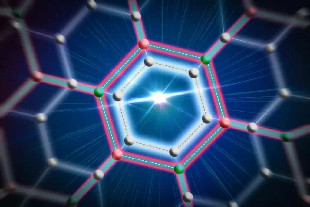
In a significant leap for the field of quantum materials science, a multidisciplinary team at the Massachusetts Institute of Technology (MIT) and several partner institutions has announced a breakthrough in the fabrication of two-dimensional superconductors. By developing a novel growth process that protects fragile materials from atmospheric degradation, the researchers have successfully integrated an air-stable, monolayer superconductor into a functional microwave circuit. This achievement, detailed in a recent publication in the journal Nature, marks a pivotal step toward the miniaturization of quantum computing hardware and the development of ultra-sensitive detectors for applications ranging from deep-space communications to cosmological observation.
The research focuses on niobium diselenide (NbSe2), a transition metal dichalcogenide that possesses remarkable superconducting properties even when reduced to a thickness of just a few atoms. Superconductors are materials that allow electricity to flow with zero resistance, a characteristic essential for the qubits (quantum bits) that power quantum computers. However, the practical application of NbSe2 has long been stymied by its extreme sensitivity to the environment. When exposed to air, the material oxidizes almost instantaneously, losing its superconducting properties and making large-scale manufacturing nearly impossible. The new MIT-led process overcomes this "oxidation barrier," allowing for the creation of wafer-scale superconducting films that remain stable in ambient conditions.
The Challenge of Two-Dimensional Superconductivity
As the global race for quantum supremacy intensifies, the physical size of quantum hardware remains a significant hurdle. Current superconducting quantum circuits often rely on bulky components to manage electrical signals and maintain coherence. Two-dimensional (2D) materials—those consisting of a single layer of atoms—offer a pathway to drastic miniaturization. Niobium diselenide is particularly prized in this context because it exhibits high kinetic inductance.
Inductance is the property of an electrical conductor by which a change in current flowing through it induces an electromotive force. In superconductors, "kinetic inductance" arises from the inertia of the charge-carrying Cooper pairs. Because NbSe2 can store a significant amount of inductive energy in an incredibly small volume, it allows engineers to replace large, complex arrays of Josephson junctions—the standard building blocks of superconducting circuits—with tiny strips of thin-film material. This could reduce the footprint of quantum processors by orders of magnitude.
Despite these advantages, the transition from laboratory curiosity to industrial component has been slow. Traditionally, researchers have produced NbSe2 through "exfoliation," a process of peeling thin layers from a bulk crystal using adhesive tape. This method produces small, irregular flakes that are insufficient for commercial semiconductor fabrication. Furthermore, even when grown using chemical vapor deposition, the material begins to degrade the moment it is removed from the vacuum chamber, requiring complex and often ineffective encapsulation techniques.
Innovation: The "Gap Growth" Methodology
The MIT team, led by graduate student Xudong Sheldon Zheng and his colleagues, pivoted away from traditional growth methods to solve the stability issue. Rather than growing the superconductor and then attempting to protect it, they developed a technique to grow the material in a pre-protected environment.
The researchers began by placing a layer of graphene—a single-atom-thick sheet of carbon—directly onto a silicon dioxide substrate. While the graphene appears to sit flush against the substrate, there is a microscopic gap between the two surfaces, measuring less than one nanometer. The team then introduced chemical precursors into this interface. Under carefully controlled conditions, the niobium diselenide crystalized within this sub-nanometer gap.
"It took a long time for us to understand how the growth could happen underneath the graphene," said Zheng, a graduate student in the MIT Department of Electrical Engineering and Computer Science (EECS). "Through collaboration and discussion, we eventually uncovered the mechanism for growing the material at the interface. This solves a lot of problems and allows us to simplify our fabrication steps."
The graphene layer serves a dual purpose: it acts as a structural template that encourages the formation of a smooth, continuous monolayer and serves as an immediate, impermeable shield against oxygen and moisture. Because the superconductor is encapsulated the moment it is formed, it can be safely removed from the growth chamber and handled in a standard cleanroom environment without the risk of degradation.
Technical Data and Experimental Results
The efficacy of this "gap growth" method was demonstrated through a series of rigorous tests. The researchers were able to produce high-quality NbSe2 films over an inch in size, a massive improvement over the micron-scale flakes produced by exfoliation.
When the team integrated the encapsulated NbSe2 into a superconducting microwave circuit, the results confirmed that the material’s intrinsic properties remained intact. The material exhibited:
- High Kinetic Inductance: The film demonstrated the ability to store inductive energy efficiently, confirming its utility for compact circuit design.
- Resilience to Fabrication: Unlike previous attempts, the material survived the etching and lithography processes required to create functional devices.
- Electrical Connectivity: One of the primary hurdles in 2D electronics is creating a "clean" electrical contact between a 1-nanometer-thick film and a 300-nanometer-thick metal electrode. The team developed a specialized side-wall etching technique in a vacuum to ensure a reliable, low-resistance connection.
By tuning the growth conditions, the researchers proved they could maintain uniform monolayer thickness across the entire substrate, a feat that has eluded the scientific community for years. This uniformity is critical for the reliable performance of quantum devices, where even slight variations in material thickness can lead to decoherence or signal loss.
Collaborative Effort and Academic Significance
The study, titled "Air-stable monolayer NbSe2 grown at the interface," represents a massive collaborative effort. Xudong Sheldon Zheng was joined by co-lead authors Sameia Zaman, an EECS graduate student, and Kenan Zhang, a former postdoc in the MIT Research Laboratory of Electronics (RLE).
The project was overseen by several corresponding authors, including William D. Oliver, the Henry Ellis Warren Professor of EECS and physics and director of the Center for Quantum Engineering at MIT. Oliver is a prominent figure in the quantum field, known for his work on the scalability of superconducting qubits. Other key contributors included Joel I-Jan Wang, an assistant professor at New York University, and Jing Kong, the Jerry McAfee Professor in Engineering at MIT.
The research also involved experts from Lincoln Laboratory, Rice University, Yale University, and Pohang University of Science and Technology in South Korea. This international cooperation underscores the global importance of the findings, as the techniques developed could be applied to a broad family of other 2D materials, such as molybdenum disulfide or tungsten ditelluride, each possessing unique electronic and optical properties.
Broader Impact: From Quantum Bits to Cosmology
The implications of this research extend far beyond the laboratory. In the short term, the ability to manufacture air-stable 2D superconductors at scale will accelerate the development of "superinductors," which are vital for a new class of qubits known as fluxonium qubits. These qubits are theorized to have longer coherence times—meaning they can stay in a quantum state longer—than the transmon qubits currently used by industry giants like IBM and Google.
In the long term, the miniaturization of these components could lead to:
- Quantum Communications: Ultrasensitive detectors based on NbSe2 could be used to pick up incredibly weak signals in quantum key distribution networks, enhancing the security of global communications.
- Cosmological Observation: The high sensitivity of these superconducting films makes them ideal candidates for the next generation of bolometers and photon detectors used in telescopes to study the cosmic microwave background radiation.
- Portable Quantum Devices: By reducing the physical size of the superconducting circuits, it may eventually become possible to create more compact quantum sensors and clocks for use in field applications where space and power are limited.
"We’ve taken a very good step toward exploring both the physics and the application side of this thin, monolayer superconductor," noted co-lead author Sameia Zaman. "There are a lot of directions we can go in the future."
Timeline and Funding
The path to this discovery was built on years of incremental progress in 2D material synthesis. The team built upon prior work regarding the "oxidation-free transfer" of materials, a technique they refined to ensure the graphene-NbSe2 structure could be moved from its growth substrate to a device substrate without damage.
The research was supported by a diverse array of funding bodies, reflecting its importance to both national security and fundamental science. Sponsors included the U.S. Army Research Office, the National Science Foundation (NSF), the U.S. Department of Energy, and the U.S. Air Force Office of Scientific Research. Additional support was provided by the Schlumberger Foundation, the Semiconductor Research Corporation, the MIT Institute for Soldier Nanotechnologies, and the National Research Foundation of Korea.
As the team looks forward, their next goal is to integrate these monolayers into more complex, multi-layered device architectures. By stacking different 2D materials, they hope to create "van der Waals heterostructures" that can perform even more advanced quantum logic operations, potentially bringing the world closer to the era of practical, large-scale quantum computing.