In a landmark development for the field of nanophotonics and quantum information science, a research team at the University of Technology Sydney (UTS) has demonstrated a sophisticated method for manipulating quantum light sources at the atomic level. By precisely twisting layers of hexagonal boron nitride (hBN), an atomically thin material often referred to as "white graphene," the researchers have successfully unlocked a new level of control over quantum emitters. This breakthrough addresses one of the most persistent challenges in quantum physics: the ability to tune and stabilize microscopic light sources that are essential for the next generation of computing, communication, and sensing technologies.
The research, led by Dr. Angus Gale and supervised by Professor Igor Aharonovich, represents a paradigm shift in how scientists interact with two-dimensional (2D) materials. While previous efforts focused on the static properties of these materials, the UTS team has introduced a dynamic "lever" that allows for the continuous modification of quantum properties through mechanical manipulation. This development is expected to accelerate the transition of quantum systems from theoretical laboratory experiments to practical, scalable industrial applications.
The Challenge of Quantum Emitters
Quantum emitters, also known as single-photon sources, are the fundamental building blocks of optical quantum technologies. Unlike conventional light sources like incandescent bulbs or LEDs, which emit a stream of billions of photons, a quantum emitter releases light one photon at a time. This characteristic is vital for quantum key distribution (QKD)—a method of secure communication that is theoretically impossible to intercept without detection—and for the gates of optical quantum computers.
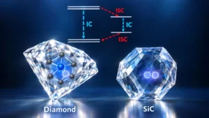
However, integrating these emitters into functional devices has proven notoriously difficult. In traditional three-dimensional semiconductors such as diamond or silicon carbide, quantum emitters are often "buried" deep within a rigid crystal lattice. While these materials have been the workhorse of quantum research for decades, their solid-state nature makes them difficult to manipulate once the device is fabricated. Researchers are often stuck with the properties the material possesses at the moment of creation, with very little room for post-production tuning.
Dr. Gale noted that while the existence of these emitters is easily verifiable through measurement, the lack of practical control has been a significant bottleneck. "You can measure these quantum emitters and see that they exist, but it’s hard to make them work in practice," Gale explained. "This gives us a lever to get closer to that—a step towards the realization of quantum technologies."
Hexagonal Boron Nitride: The "Cheese Slice" Advantage
The UTS team turned to hexagonal boron nitride (hBN) to solve the rigidity problem. Hexagonal boron nitride is a van der Waals material, meaning it consists of layers held together by weak intermolecular forces rather than strong chemical bonds. This structure allows the material to be exfoliated into sheets that are only a few atoms thick.
To illustrate the unique properties of hBN, Dr. Gale employed a culinary analogy, comparing the material to slices of cheese rather than a solid block. "With a block of cheese, you can’t really get to the flavor in the middle. But with slices, you can peel away layers, put them back together, and change how they interact," he said.
In traditional materials like diamond, a defect (the source of the quantum light) is trapped in a 3D matrix. In hBN, the defect resides within a 2D plane. By stacking two or more of these planes and rotating them relative to one another—a field of study known as "twistronics"—researchers can alter the local electronic environment surrounding the emitter. This interaction directly influences the energy levels of the quantum source, thereby changing the characteristics of the light it produces.
Experimental Breakthroughs and Observations
The UTS experiments focused on the magnitude of change achievable through twisting. The team discovered that by rotating the hBN layers, they could significantly alter both the color and the wavelength of the emitted light. In the realm of quantum optics, even minor shifts in wavelength are critical, but the UTS team observed shifts that were much larger than initially anticipated.
One of the most innovative aspects of the study was the repeatability of the process. In typical twistronics experiments, a device is fabricated at a specific angle and remains in that configuration. The UTS researchers, however, developed a methodology to repeatedly lift, rotate, and restack the material. This "dynamic tuning" allowed them to observe the evolution of the light source in real-time as the twist angle changed.
"The benefit is that we used this twistable platform to shift the emission by a very significant amount," Gale stated. "Often when you control these systems, the amount of manipulation is very limited, but in this case, the shift was much larger than expected. Rather than trying to make hBN defects behave like traditional solid-state hosts, we took advantage of hBN’s own strength: its thin, layered, twistable structure."
The Physics of Twistronics and Moiré Patterns
The underlying physics of this discovery is tied to the formation of Moiré patterns. When two periodic lattices are overlaid with a slight twist or a difference in lattice constant, they create a new, larger periodic interference pattern. This Moiré superlattice creates a new potential energy landscape for electrons and photons.
In the case of hBN, the twist changes the strain and the electronic coupling between the layers. Because the quantum emitters in hBN are typically point defects—missing atoms or substituted atoms within the lattice—they are highly sensitive to these local changes. The UTS team’s ability to manipulate this environment via twisting essentially allows them to "tune" the emitter’s frequency, similar to how one might tune a radio to a specific station.
This level of control is particularly exciting for Professor Igor Aharonovich, the supervising author of the study and a leading figure in the world of nanophotonics. "You can take two layers that don’t do much on their own, put them together at a specific angle, and suddenly you have a completely different system," Aharonovich said.
Implications for Future Technology
The ability to tune quantum light sources has far-reaching implications across several high-tech sectors. As quantum technology moves out of the lab and into the real world, the demand for reliable, tunable, and scalable components will only grow.
Quantum Computing and Communication
In quantum computing, photons are used to carry information between different parts of a processor or between separate quantum computers in a network. For these systems to work, the photons must be indistinguishable—meaning they must have the exact same wavelength and phase. The UTS discovery provides a mechanism to "match" emitters that might otherwise have slightly different properties, ensuring they can work together in a unified system.
In the realm of cybersecurity, this technology could bolster Quantum Key Distribution (QKD). By having more control over the emission properties, scientists can create more efficient and secure communication links that are immune to traditional hacking methods.
Healthcare and Bio-Sensing
Quantum sensors are another major area of application. Because quantum states are incredibly sensitive to their environment, they can be used to measure magnetic fields, temperature, or chemical concentrations with unprecedented precision. Tunable hBN emitters could lead to the development of nano-scale sensors capable of monitoring biological processes inside a single cell, potentially revolutionizing drug discovery and medical diagnostics.
Navigation and GPS
The precision offered by quantum systems can also enhance global positioning systems. Current GPS relies on atomic clocks; however, quantum-enhanced sensors could provide even more accurate timing and positioning data, which is essential for autonomous vehicles and advanced aerospace applications.
Strategic Context: Australia’s Role in the Quantum Race
The research conducted at UTS is part of a broader global effort to achieve "quantum supremacy" and commercialize quantum-based tools. Australia has emerged as a significant player in this field, with the federal government recently launching the National Quantum Strategy to foster innovation and investment.
The UTS study highlights the importance of materials science in the quantum roadmap. While much of the public discourse centers on the "qubits" themselves, the underlying materials—and the ability to engineer them at the atomic scale—are what will ultimately determine the feasibility of these technologies.
Conclusion and Future Outlook
The work of Dr. Gale, Professor Aharonovich, and their team at the University of Technology Sydney provides a vital new tool for the quantum toolkit. By moving away from the rigid structures of the past and embracing the flexible, layered nature of 2D materials, they have demonstrated that "twisting" is not just a physical action, but a powerful engineering principle.
The next steps for the research will likely involve integrating these twistable hBN layers into integrated photonic circuits. If the team can automate the twisting and tuning process on a microchip, it would pave the way for mass-produced quantum devices.
As Professor Aharonovich concluded, "These materials could eventually be used for quantum computing communications and quantum sensing, which would help for applications such as healthcare, cybersecurity, and improved GPS; and gives us more control over the building blocks needed to get there."
With this new "lever" in hand, the scientific community is one step closer to a future where quantum technology is a ubiquitous part of modern infrastructure, providing security, precision, and computing power that was once the stuff of science fiction.