The global push for sustainable technology has reached a pivotal milestone as researchers at Chalmers University of Technology in Sweden announce a breakthrough in the field of superconductivity, potentially paving the way for a new era of ultra-efficient electronics. By developing a novel method to stabilize superconductivity at higher temperatures and under intense magnetic fields, the team has addressed two of the most persistent technical hurdles that have historically confined these materials to specialized laboratory settings. The study, recently published in the prestigious journal Nature Communications, suggests that the future of power grids, quantum computers, and high-speed communications may rely not just on the materials themselves, but on the precise engineering of the surfaces upon which they are built.
Superconductors represent a holy grail in materials science due to their ability to conduct electricity with zero resistance. In a world where modern digital infrastructure, ranging from massive data centers to sprawling information and communications technology (ICT) networks, accounts for between 6 and 12 percent of total global electricity consumption, the implications of zero-loss energy transmission are profound. Current electronic systems suffer from Joule heating—the process by which energy is lost as heat when electrons collide with atoms in a conductor. Superconductors eliminate this waste, offering a theoretical pathway toward devices that are hundreds of times more efficient than current silicon-based technologies.
The Persistent Challenges of Superconductivity
Despite the discovery of superconductivity over a century ago, its practical application has been hampered by extreme environmental requirements. Traditionally, most superconducting materials only exhibit their unique properties at temperatures approaching absolute zero. Even the so-called "high-temperature" superconductors, discovered in the 1980s, typically require cooling to approximately minus 200 degrees Celsius, necessitating expensive and bulky liquid nitrogen or liquid helium cooling systems.
Beyond the "temperature wall," researchers have long struggled with the "magnetic wall." Superconductivity is a delicate state of matter characterized by the formation of Cooper pairs—pairs of electrons that move in unison. Strong magnetic fields can penetrate the material and disrupt these pairs, effectively "turning off" the superconducting state. This vulnerability is particularly problematic because many of the most promising applications for superconductors, such as Magnetic Resonance Imaging (MRI) machines, fusion reactors, and quantum processors, involve or generate powerful magnetic environments.
For decades, the primary strategy for improving these materials focused on chemical doping—the process of adding or substituting atoms within the material’s crystal lattice to alter its electronic properties. However, this approach has reached a point of diminishing returns, particularly with complex materials like cuprates, which are notoriously brittle and chemically stubborn.
A Paradigm Shift: Engineering the Interface
The team at Chalmers University, led by Floriana Lombardi, Professor of Quantum Device Physics, decided to bypass the limitations of chemical modification by focusing on the physical interface where the superconductor meets its supporting environment. Instead of trying to change what the material is made of, they changed how the material sits on its foundation, known as the substrate.
The researchers utilized a specific type of high-temperature superconductor belonging to the cuprate family: Yttrium Barium Copper Oxide (YBCO). These materials are known for their high transition temperatures but are incredibly sensitive to their structural environment. The superconducting layer used in the Chalmers experiment was an "ultrathin" film, measuring only a few nanometers in thickness—roughly one-thousandth the thickness of a human hair.
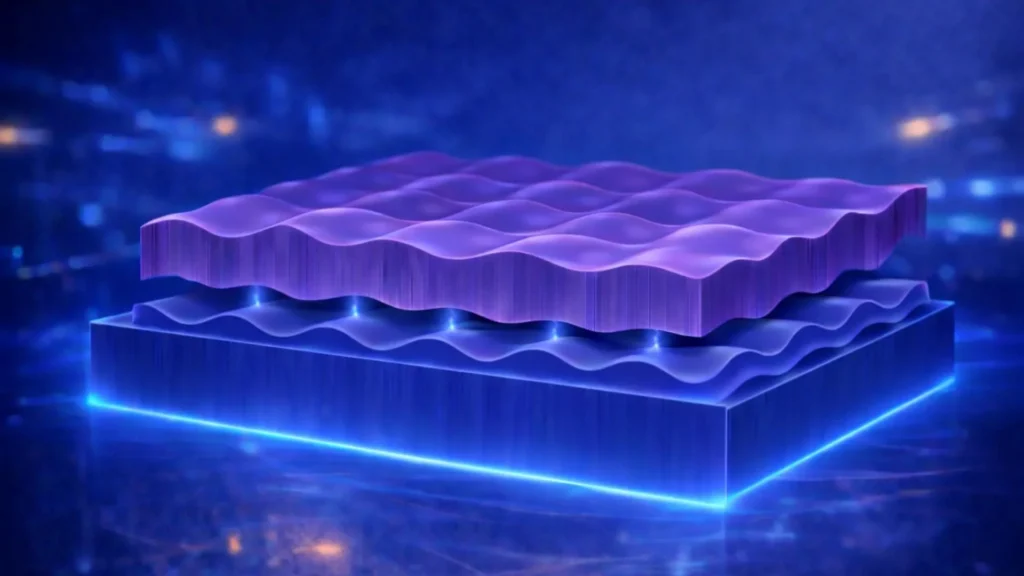
The breakthrough involved the creation of a "nanofaceted" substrate. Before the superconducting film was deposited, the researchers treated the substrate surface in a high-temperature vacuum environment. This process caused the surface of the substrate to reorganize into a highly ordered pattern of microscopic ridges and valleys.
"By sculpting the surface that the superconductor rests on, we were able to induce superconductivity at significantly higher temperatures than previously possible," explained Professor Lombardi. "We also found that the material remained superconducting even when exposed to strong magnetic fields."
The Science of Atomic Alignment
The success of the nanofaceted substrate lies in the concept of epitaxial growth. When a thin film is grown on a substrate, the atoms of the film tend to align themselves with the pattern of the atoms in the foundation. By creating a specific "corrugated" geometry on the substrate, the Chalmers team forced the YBCO atoms to settle into a configuration that optimized the flow of electrons.
Eric Wahlberg, a researcher at the RISE Research Institutes of Sweden and a key contributor to the study, noted that the atomic arrangement of the substrate serves as a template. The ridges and valleys on the surface created a specific electronic environment at the interface—the point where the two materials touch. This interface altered the behavior of the electrons, giving them a "preferential direction" that stabilized the superconducting state against external disruptions.
Data from the study indicates that this structural "nudging" allowed the thin films to maintain their zero-resistance state at temperatures higher than those achieved with flat, non-engineered substrates. More importantly, the engineered films showed a remarkable resilience to magnetic fields that would typically quench superconductivity in standard cuprate samples. This suggests that the interface engineering effectively "pins" the superconducting state, making it more robust against the magnetic vortices that usually lead to energy dissipation.
Chronology of the Research and International Collaboration
The development of this technique was the result of a multi-year effort involving a diverse coalition of international experts. The project began with theoretical modeling to predict how surface geometry might influence electron pairing in cuprates. This was followed by rigorous experimentation at Myfab Chalmers, a world-class cleanroom facility that allows for the manipulation of materials at the atomic scale.
The research timeline involved:
- Initial Surface Analysis: Developing the vacuum-heat treatment protocols to create consistent nanofacets on the substrate.
- Film Deposition: Using pulsed laser deposition to grow YBCO films atom-by-atom onto the faceted surfaces.
- Cryogenic Testing: Subjecting the samples to extreme cold and high-intensity magnetic fields to map the limits of their performance.
- Data Verification: Collaborative analysis involving researchers from Sweden, Italy, France, Germany, and India to confirm that the observed boost in performance was indeed a result of the surface geometry.
The findings were co-authored by a team including Riccardo Arpaia, Debmalya Chakraborty, and Alexei Kalaboukhov, among others. The project received significant backing from the Swedish Research Council, the Knut and Alice Wallenberg Foundation, and the European Union’s EIC Pathfinder grant, reflecting the high strategic importance of this research for the continent’s technological sovereignty.
Broad Implications for Quantum Technology and the Energy Sector
The implications of this research extend far beyond the laboratory. In the realm of quantum computing, the stability of qubits—the basic units of quantum information—is paramount. Many quantum architectures rely on superconducting circuits. If these circuits can be made more resilient to magnetic interference and operate at slightly higher temperatures, it could drastically reduce the complexity and cost of quantum hardware, bringing the "quantum advantage" closer to reality.
In the energy sector, the potential for high-field, high-temperature superconductors could revolutionize the power grid. High-voltage direct current (HVDC) lines using these engineered superconductors could transport electricity across continents with zero loss, a critical requirement for integrating remote renewable energy sources like offshore wind or desert solar farms into urban grids.
Furthermore, the "design principle" introduced by the Chalmers team—focusing on substrate geometry rather than chemistry—provides a new roadmap for materials science. This approach could potentially be applied to other classes of materials, such as topological insulators or 2D materials like graphene, to unlock properties that are currently suppressed by structural disorder.
Expert Analysis and Future Outlook
Industry analysts suggest that while commercial application is still years away, the Chalmers study provides a "proof of concept" that could shift how the electronics industry approaches miniaturization. As transistors approach the physical limits of silicon, the heat generated by traditional conductors becomes a barrier to further performance gains. Superconducting thin films, stabilized by nanofaceted substrates, offer a way to continue the trajectory of Moore’s Law without the thermal penalty.
"This shows that very small changes at the nanoscale can have decisive effects," Lombardi stated. The research team now aims to test this method on other superconducting materials and explore whether even more complex surface patterns could push the transition temperature closer to room temperature—the ultimate goal of the field.
As the global community grapples with the twin challenges of increasing digital demand and the need for energy decarbonization, the work at Chalmers University stands as a testament to the power of precision engineering. By looking at the surface of the problem, these scientists may have found the key to unlocking the full potential of one of nature’s most mysterious and promising phenomena.
The study, "Boosting superconductivity in ultrathin YBa2Cu3O7−δ films via nanofaceted substrates," serves as a definitive marker in the transition from fundamental physics to applied superconducting engineering. With the blueprint for stronger superconductivity now established, the race to integrate these materials into the next generation of global infrastructure has entered a new and more promising phase.