For decades, ultrafast lasers have stood as formidable instruments within the realm of modern optics, their capabilities defined by pulses lasting mere hundreds of femtoseconds—quadrillionths of a second. These ephemeral bursts of light have been the bedrock for a diverse array of advanced technologies, from the meticulous demands of precision manufacturing and intricate eye surgery to the groundbreaking innovation of optical frequency combs, a Nobel Prize-winning advancement that underpins the world’s most accurate optical atomic clocks. Yet, despite their profound utility and impact across scientific and industrial landscapes, these powerful tools have remained largely confined to laboratories, characterized by their substantial size and prohibitive cost, often occupying entire optical tables.
A Breakthrough in Miniaturization
The long-standing challenge of miniaturizing these indispensable systems has now been addressed by a team of researchers led by Professor Tobias J. Kippenberg at EPFL (École Polytechnique Fédérale de Lausanne). Their work, recently published in the prestigious journal Nature, details a significant breakthrough: the development of the first integrated ultrafast laser capable of matching the performance metrics traditionally associated with large-scale, tabletop femtosecond lasers. This novel device delivers impressive pulse energies of 1.05 nanojoules and achieves pulse durations as brief as 147 femtoseconds, all from a compact photonic chip. This achievement heralds a potential revolution, promising to dramatically shrink the footprint and cost of ultrafast laser technology, thereby democratizing access to its transformative capabilities.
The Enduring Legacy and Challenge of Ultrafast Lasers
The journey of ultrafast lasers began in the 1960s with the advent of mode-locked lasers, which enabled the generation of picosecond (trillionths of a second) pulses. Over the subsequent decades, continuous innovation, particularly with the development of Kerr-lens mode-locking in the late 1980s and early 1990s, pushed pulse durations into the femtosecond regime. These advancements unlocked unprecedented control over light-matter interactions, opening new frontiers in fields ranging from fundamental physics to advanced medicine.
To fully appreciate the brevity of a femtosecond, consider this: a femtosecond is to one second what one second is to approximately 31.7 million years. This extreme temporal resolution allows scientists to observe and manipulate ultrafast phenomena, such as chemical reactions and electron dynamics, that occur on timescales previously inaccessible. In industrial applications, the extremely short pulse duration and high peak power of femtosecond lasers enable "cold ablation," a process where material is removed with minimal heat diffusion into the surrounding area. This precision is critical for manufacturing microelectronics, creating stents, or performing delicate surgical procedures with sub-micron accuracy.
Optical frequency combs, recognized with the Nobel Prize in Physics in 2005 for John L. Hall and Theodor W. Hänsch, are perhaps one of the most sophisticated applications. These combs act as "optical rulers," providing a precise spectrum of equally spaced, sharply defined laser frequencies. They have revolutionized precision spectroscopy, enabling ultra-accurate measurements of atomic and molecular transitions, facilitating the search for exoplanets by detecting minute stellar wobbles, and most notably, serving as the timing mechanism for the world’s most accurate optical atomic clocks, which lose less than one second in billions of years.
However, the very complexity and power that make these lasers so valuable have also contributed to their bulk. Traditional tabletop femtosecond lasers typically involve an intricate arrangement of discrete optical components—mirrors, lenses, prisms, and gain media—spread across optical benches that can span several square meters. They require precise alignment, temperature control, and often powerful cooling systems, making them susceptible to environmental vibrations and thermal fluctuations. Consequently, their acquisition and operational costs can easily run into the hundreds of thousands to millions of dollars, severely limiting their widespread deployment beyond specialized research institutions and high-end industrial facilities. The dream of integrating such powerful tools into portable, cost-effective devices has, for over two decades, been considered a "holy grail" in integrated photonics, a goal now brought significantly closer by the EPFL team.
Integrated Photonics: The Foundation for Miniaturization
The field of integrated photonics aims to manipulate light using microscopic structures etched onto a wafer, much like electronic chips process electrical signals. These "photonic chips" guide and process light through tiny waveguides, analogous to wires in electronic circuits. This technology has already proven transformative in telecommunications, enabling the miniaturization of optical transceivers and other components that were once large and cumbersome.
The platform chosen by the EPFL researchers for their integrated ultrafast laser is silicon nitride (SiN). SiN is a material highly valued in integrated photonics due to its low optical loss, high nonlinearity, and compatibility with standard CMOS manufacturing processes, which allows for mass production at wafer scale. This compatibility is a critical factor for reducing costs and increasing accessibility, drawing parallels to the revolution brought about by silicon microelectronics.
"For more than twenty years, a high-pulse-energy femtosecond laser on chip was widely regarded as a holy grail of integrated photonics," remarked Professor Kippenberg. "Our result shows that it is not only possible, but that it can be achieved with a surprisingly elegant architecture that the integrated-photonics community had overlooked." This statement underscores the profound impact of their work, not just in achieving a technical milestone but also in demonstrating a novel architectural approach.
The Elegance of the Mamyshev Oscillator
To achieve this feat, the researchers adopted a laser architecture known as the Mamyshev oscillator. This design, while known in the broader laser community, had received relatively little attention within the integrated photonics sector. Its ingenious simplicity and robustness proved perfectly suited for the constraints and opportunities presented by a chip-based platform.
The core of the Mamyshev oscillator system involves placing a nonlinear waveguide between two optical filters. Each filter is specifically designed to transmit a different, narrow portion of the light spectrum. The operation is self-regulating: as an intense laser pulse travels through the nonlinear waveguide, it undergoes self-phase modulation, a nonlinear optical effect that causes its spectrum to broaden, expanding into a wider range of colors. Crucially, only the central, broadened portion of this pulse can then pass through both filters, allowing it to continue circulating within the laser cavity and reinforce itself.
Weaker light, conversely, behaves differently. Because its intensity is insufficient to induce significant spectral broadening, it cannot pass through both filters and is effectively blocked and removed from the laser cycle. This mechanism acts as a robust form of mode-locking, ensuring that only strong, well-formed pulses are sustained, while noise and weaker light are suppressed.
Zheru Qiu, a co-leading author of the paper, elaborated on the practical advantages of this design: "This design is especially attractive because it does not require any component that is difficult to make on this erbium-doped silicon nitride chip." This is a critical point for integrated photonics, where the complexity of fabricating individual components can significantly impact manufacturing feasibility and cost. The use of erbium doping provides the necessary optical gain for the laser, a standard technique integrated into the SiN platform.
Qiu further highlighted another major benefit. Integrated photonic chips inherently confine light to extremely small waveguides. This tight confinement leads to strong light-matter interactions and enhanced nonlinear effects. While these nonlinearities are essential for the Mamyshev oscillator’s operation, in many other laser architectures, uncontrolled or excessive nonlinear effects can destabilize laser pulses, leading to poor performance or even system failure. The Mamyshev oscillator, however, is remarkably less susceptible to these destabilizing problems, making it an ideal candidate for integrated photonic devices where nonlinearities are often amplified due to the confined optical fields.
Miniature Device, Monumental Potential
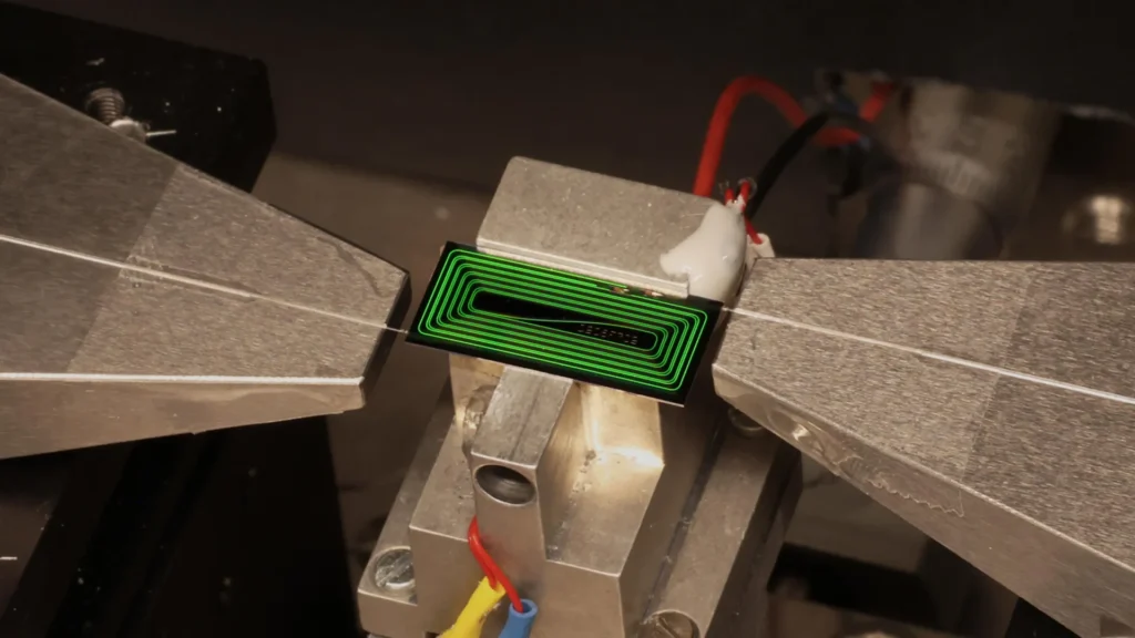
The physical dimensions of this groundbreaking integrated laser are astonishing. The laser cavity, which is 42 centimeters in length when unraveled, is ingeniously folded onto a chip occupying an area roughly the size of a match head. This makes it dramatically smaller than conventional fiber-based ultrafast lasers, let alone their bulkier tabletop counterparts. This reduction in size is not merely an aesthetic achievement; it translates directly into portability, reduced power consumption, and enhanced robustness.
The manufacturing implications are equally significant. Because photonic chips can be produced at wafer scale using methodologies akin to those employed for computer chips (e.g., lithography, etching), the potential for mass production is immense. More than 1,000 laser cavities could theoretically be manufactured simultaneously on a single wafer. This manufacturing advantage stands to significantly reduce the per-unit cost of ultrafast lasers, moving them from niche, expensive laboratory instruments to widely accessible tools.
This cost reduction and expanded availability will, in turn, unlock a cascade of new applications. "With kilowatt-level peak powers, the chip can drive demanding applications that have long depended on large, expensive laboratory lasers," Qiu noted. This speaks to the functional equivalence of the integrated device to its larger predecessors, overcoming a key hurdle in integrated photonics—maintaining performance despite miniaturization.
Transformative Applications and Future Trajectories
The researchers envision a future where this technology leads to a new generation of portable and affordable devices that will impact numerous sectors:
- Environmental Monitoring: Compact, high-sensitivity ultrafast lasers could enable real-time, on-site detection of environmental pollutants, greenhouse gases, and airborne toxins. Imagine handheld devices for identifying hazardous substances or distributed sensor networks for monitoring air quality across urban environments with unprecedented precision.
- Material Science and Industrial Inspection: The ability to perform non-destructive testing with extreme precision could revolutionize quality control in manufacturing. These lasers could identify hidden defects, micro-cracks, or structural weaknesses in materials ranging from aerospace components to semiconductor wafers, ensuring higher reliability and safety.
- Medical Diagnostics and Therapeutics: The prospect of portable and affordable ultrafast lasers could lead to advancements in point-of-care diagnostics, bringing sophisticated medical imaging techniques like optical coherence tomography (OCT) out of specialized clinics and into general practitioners’ offices or even ambulances. Furthermore, their precision could enhance existing surgical techniques, leading to less invasive procedures and faster patient recovery.
- Communications and Navigation: The miniaturization of components for optical atomic clocks is particularly exciting. These compact, robust clocks could play critical roles in next-generation global positioning systems (GPS), providing even greater accuracy and resilience. They could also underpin advanced secure communication networks and contribute to the foundational infrastructure for quantum computing.
- Scientific Research: By making ultrafast laser technology more accessible and affordable, this breakthrough has the potential to democratize scientific discovery. Researchers in smaller labs or developing countries could gain access to tools previously out of reach, fostering innovation across chemistry, biology, and physics.
The work, a collaborative effort involving researchers from the EPFL Institute of Electrical and Microengineering and Helmholtz-Zentrum Dresden-Rossendorf (HZDR), represents not just a technical triumph but a strategic shift in how high-performance optical tools can be conceived, manufactured, and deployed. While the current research demonstrates the feasibility and performance, future work will likely focus on further integration, packaging, and developing specific application-driven systems. The journey from laboratory breakthrough to widespread commercial adoption is often complex, but this achievement lays a robust foundation for a future where the unparalleled power of ultrafast light is no longer confined to the lab, but is ubiquitous, empowering new innovations across society.