For decades, the relentless pursuit of smaller and more powerful electronic components has been the primary engine driving monumental advancements across all facets of technology, from supercomputers to smartphones. As the silicon-based microelectronics industry approaches fundamental physical limits, the search for the next paradigm-shifting breakthrough in computer chip design has intensified, with many researchers positing that two-dimensional (2D) materials could hold the key. These ultrathin materials, characterized by their composition of merely one or a few atomic layers, have garnered significant attention as highly promising candidates for constructing the next generation of even tinier and more efficient electronic devices. Their unique properties, including exceptional electronic mobility, tunable bandgaps, and mechanical strength, have fueled extensive global research and development efforts.
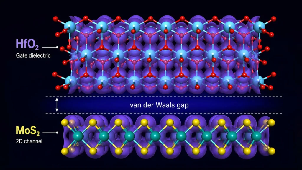
However, groundbreaking new research originating from TU Wien in Austria casts a critical light on this optimistic outlook, suggesting that many of these highly touted 2D materials may not perform as anticipated when integrated into real-world chip technology. The problem, as identified by the TU Wien team, transcends the intrinsic properties of the 2D material itself. Scientists discovered that when 2D materials are paired with the essential insulating layers—also known as dielectrics—required for the functional operation of electronic devices, an unavoidable, atomic-scale gap invariably forms between them. This minute, yet profoundly significant, separation can drastically reduce device performance and, crucially, establishes a fundamental physical barrier to further miniaturization, challenging long-held assumptions in the field. The implications of these findings are substantial, potentially helping the multi-billion-dollar semiconductor industry to avoid investing vast sums in research and development approaches that, due to these newly identified physical limitations, may ultimately prove to be dead ends.
The Relentless March of Miniaturization: From Vacuum Tubes to Nanoscale Transistors
The history of modern computing is inextricably linked to the principle of miniaturization, famously encapsulated by Moore’s Law. First articulated by Intel co-founder Gordon Moore in 1965, this observation predicted that the number of transistors on an integrated circuit would double approximately every two years. For over half a century, this exponential growth held true, driving unprecedented leaps in computational power, energy efficiency, and cost reduction. Early computers, reliant on bulky vacuum tubes, quickly gave way to devices built with discrete transistors, which were then supplanted by integrated circuits fabricated on silicon wafers. Silicon, a naturally abundant semiconductor, proved to be an almost ideal material for transistor fabrication due to its excellent electrical properties, robust processing capabilities, and the ability to form a stable, high-quality insulating layer (silicon dioxide).
The constant shrinking of transistors, from micrometers to nanometers, has enabled the proliferation of sophisticated electronic devices that define our modern world. However, as transistor features approach atomic scales—currently in the single-digit nanometer range—silicon-based technology faces increasingly formidable challenges. Quantum mechanical effects, such as electron tunneling, become more pronounced, leading to increased leakage currents and power consumption. Heat dissipation becomes a critical bottleneck, limiting clock speeds and packaging density. Furthermore, the immense capital expenditure required to build and operate advanced fabrication facilities (fabs) for sub-10nm nodes has become astronomical, creating economic pressures that rival the physical ones. These escalating challenges have spurred a global quest for "beyond silicon" materials and architectures, aiming to sustain the trajectory of technological progress.
The Promise and Peril of 2D Materials
In this intensive search for alternatives, 2D materials emerged as leading candidates, sparking immense excitement across the scientific community. Graphene, discovered in 2004, was the first 2D material to capture widespread attention due to its extraordinary properties: exceptional electron mobility (faster than silicon), mechanical strength (200 times stronger than steel), and thermal conductivity. Following graphene’s discovery, a veritable "zoo" of other 2D materials has been identified and studied, each possessing unique characteristics suitable for various applications. Molybdenum disulfide (MoS2), for instance, is a transition metal dichalcogenide (TMD) that exhibits a direct bandgap, making it suitable for logic transistors and optoelectronic devices, unlike graphene which is a semimetal. Hexagonal boron nitride (hBN) serves as an excellent atomically thin insulator, often used in van der Waals heterostructures.
The appeal of these materials for next-generation electronics is multifaceted. Their atomic thinness offers the ultimate limit of miniaturization, potentially allowing for denser integration of components. Their surface-dominated properties promise enhanced gate control, while their unique electronic band structures open doors to novel functionalities. Researchers envisioned building transistors where the channel material could be just a few atoms thick, dramatically reducing power consumption and increasing switching speeds. Investments poured into academic and industrial research labs globally, with governments and corporations recognizing the potential for these materials to revolutionize computing, sensing, and energy technologies. The global market for 2D materials, though nascent, was projected to grow significantly, reflecting the anticipation of their eventual integration into commercial products.
Why Interfaces Matter: The Crucial Role of Dielectrics
"For many years, researchers have quite rightly been fascinated by the remarkable electronic properties of novel 2D materials such as graphene or molybdenum disulfide," explains Prof. Mahdi Pourfath, who led the research alongside Prof. Tibor Grasser at TU Wien’s Institute for Microelectronics. "What is often overlooked, however, is that a 2D material alone does not make an electronic device. We also need an insulating layer – usually an oxide. And this is where things become more complicated from a materials science perspective."
Modern field-effect transistors (FETs), the fundamental building blocks of digital electronics, operate by switching a semiconductor channel between conductive (ON) and nonconductive (OFF) states. This switching action is controlled by a gate electrode, which must be electrically isolated from the active semiconductor material by a dielectric (insulating) layer. This insulating layer, often referred to as a gate dielectric, is critical for several reasons: it prevents current leakage between the gate and the channel, allows for effective capacitive coupling between the gate voltage and the channel charge, and helps maintain device stability. In the context of future chips employing ultrathin 2D materials as the semiconductor channel, the gate dielectric layer also needs to be exceptionally thin to maximize gate control and minimize operating voltages, thereby ensuring high performance and energy efficiency.
The TU Wien team’s breakthrough lies in meticulously examining the atomic-scale interactions at this critical interface. Their findings indicate that while the individual properties of 2D materials are impressive, the interaction (or lack thereof) with the necessary insulating layers presents a formidable, often overlooked, challenge.
The Tiny Gap Creating a Big Problem: Van der Waals Weakness
"In many combinations of 2D materials and insulating layers, the bonding between them is relatively weak," explains Grasser. "They are held together only by so-called van der Waals forces, which provide only a weak attraction between the semiconductor and the insulator. As a result, the two layers do not come into close contact – there is always a gap between them."
Van der Waals forces are weak, short-range intermolecular forces that arise from temporary fluctuations in electron distribution, creating transient dipoles. While these forces are crucial for holding together many layered materials (like graphite) and for biological interactions, they are inherently weak compared to covalent or ionic bonds. When a 2D material, such as MoS2, is physically placed on top of a conventional high-k dielectric like hafnium dioxide (HfO2) or aluminum oxide (Al2O3)—materials commonly used as gate dielectrics in advanced silicon chips—these weak van der Waals forces are often the primary means of adhesion.
The consequence, as precisely quantified by the TU Wien researchers, is the formation of an unavoidable, albeit minuscule, physical gap. This separation typically measures approximately 0.14 nanometers (nm). To put this into perspective, this gap is thinner than a single sulfur atom (atomic radius ~0.10 nm) and roughly 700 times smaller than the diameter of a SARS-CoV-2 virus particle (~70-90 nm). Despite its infinitesimal size, this gap has a dramatic and detrimental effect on the electronic behavior of the device.
"This gap weakens the capacitive coupling between the layers. No matter how good the intrinsic properties of the materials may be, the gap can become the limiting factor. As long as it exists, it imposes a fundamental limit on how far these devices can be miniaturized," Grasser emphasizes. Capacitive coupling is the efficiency with which the gate electrode’s electric field can modulate the charge carriers in the semiconductor channel. A weakened coupling means that a larger gate voltage is required to switch the transistor, or that the switching speed is reduced. This directly translates to higher power consumption, slower operation, and diminished overall device performance, thereby undermining the very advantages that 2D materials were expected to deliver for ultimate miniaturization. The research underscores that focusing solely on the impressive intrinsic properties of 2D materials, without adequately considering these critical interface effects, has led many studies down a potentially misleading path.
Implications for the Semiconductor Industry: Billions at Stake
The findings from TU Wien carry profound implications for the global semiconductor industry, an industry projected to exceed $1 trillion in market value by 2030, and one that invests billions annually into research and development. Major players like Intel, TSMC, Samsung, and IBM continually pour resources into exploring next-generation materials and architectures to maintain their competitive edge and continue the pace of technological innovation. A significant portion of this investment has been directed towards 2D materials research, including efforts in material synthesis, device fabrication, and integration strategies.
The TU Wien research serves as a stark warning: without addressing this fundamental physical limitation, a substantial portion of these investments could be misdirected. It highlights the risk of pursuing miniaturization strategies based on 2D materials that are fundamentally hampered by interface issues. Industry analysts, while generally optimistic about advanced materials, have often cautioned about the significant engineering challenges associated with integrating novel materials into existing fabrication processes. This research provides a concrete, atomic-scale physical mechanism for one such major challenge, demanding a strategic re-evaluation of current research trajectories.
The findings are likely to prompt semiconductor giants to re-prioritize research into interface engineering and novel dielectric integration methods. It underscores the necessity for a holistic approach to material selection and device design, moving beyond the isolated study of individual component properties. For companies that have made significant bets on 2D materials, this research could necessitate a pivot in their R&D focus, emphasizing collaborative design between material scientists specializing in 2D materials and those expert in dielectric integration.
"Zipper Materials" Could Offer a Solution: A Path Forward
Despite identifying a significant hurdle, the TU Wien research is not solely a cautionary tale; it also points towards a viable solution. "If the semiconductor industry wants to succeed with 2D materials, the active layer and the insulating layer must be designed together from the very beginning," emphasizes Mahdi Pourfath.
One promising answer lies in the concept of "zipper materials." In these systems, the 2D semiconductor and the insulating layer are engineered to bond together much more strongly than through weak van der Waals forces. Instead, they form robust chemical bonds—either covalent or ionic—creating a truly intimate atomic interface without any intervening gap. This tighter connection effectively "zips" the layers together, eliminating the problematic separation and restoring efficient capacitive coupling.
Achieving this strong bonding requires careful material selection and advanced fabrication techniques. It might involve designing 2D materials with specific surface functionalizations that can readily react with the dielectric, or identifying novel dielectric materials that can form strong, direct chemical bonds with the 2D semiconductor at the atomic scale. Examples could include certain oxides or nitrides grown epitaxially or through atomic layer deposition (ALD) processes that facilitate direct bond formation. This approach demands a paradigm shift in material synthesis and integration, moving away from simply stacking disparate materials to co-designing the entire interface from the atomic level upwards.
"Our work is good news for the semiconductor industry," says Tibor Grasser. "We can predict which materials are suitable for future miniaturization steps – and which are not. But if one focuses only on the 2D materials themselves, without considering the unavoidable insulating layers from the outset, there is a risk of investing billions in an approach that simply cannot succeed for fundamental physical reasons." This perspective transforms the identified problem into a crucial guiding principle for future research, offering a clear roadmap for selecting and engineering material systems that possess the inherent compatibility required for advanced electronic devices.
Broader Landscape of Advanced Materials Research
The TU Wien findings contribute to a broader understanding of the challenges and opportunities in advanced materials research for electronics. While 2D materials hold immense promise, their integration into complex circuits involves overcoming numerous hurdles beyond just the dielectric interface. These include developing scalable manufacturing techniques for large-area, high-quality 2D films, achieving precise doping control to tune electrical properties, managing thermal dissipation in ultrathin structures, and ensuring long-term device stability and reliability.
The concept of van der Waals heterostructures, where different 2D materials are stacked layer-by-layer like molecular Lego bricks, has been a major research focus. The TU Wien work indicates that even within these carefully constructed heterostructures, the interfaces with non-2D components (like gate dielectrics or metal contacts) remain critical points of failure or performance limitation.
Globally, governments are heavily investing in semiconductor research and manufacturing, recognizing its strategic importance for economic competitiveness and national security. Initiatives like the CHIPS and Science Act in the United States and the European Union’s Chips Act aim to bolster domestic capabilities in advanced chip technology. Research like that from TU Wien is vital for guiding these massive investments, ensuring that public and private funds are directed towards scientifically sound and technologically feasible pathways. The insights gained will not only influence the future of logic transistors but also have implications for 2D material applications in memory devices, advanced sensors, and even emerging fields like quantum computing, where precise control over atomic-scale interfaces is paramount.
In conclusion, the research from TU Wien provides a critical scientific anchor in the turbulent waters of next-generation chip development. By precisely identifying the atomic-scale gap and its detrimental effects on 2D material-based devices, the team has illuminated a fundamental physical barrier to further miniaturization. Yet, by simultaneously proposing solutions like "zipper materials" and advocating for a holistic co-design approach, they have also charted a clearer, more informed path forward. This work underscores the enduring importance of fundamental materials science research in guiding industrial innovation and ensuring that the relentless march of technological progress continues, built on a solid foundation of physical understanding.