For decades, ultrafast lasers have stood as indispensable powerhouses in modern optics, their fleeting pulses, lasting mere hundreds of femtoseconds—quadrillionths of a second—underpinning a remarkable array of advanced technologies. From the meticulous precision required in modern manufacturing and intricate eye surgeries to the foundational innovation of optical frequency combs, which earned a Nobel Prize and now drive the world’s most accurate optical atomic clocks, the influence of these lasers is pervasive. However, their critical role has historically been tethered to a significant drawback: they have remained predominantly large, costly, and complex systems, typically occupying entire optical tables within specialized laboratories. This inherent bulkiness and expense have severely limited their widespread deployment and integration into more compact, accessible applications.
The Dawn of a New Era in Photonics
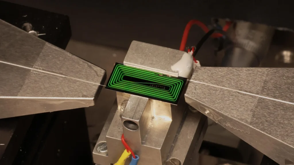
A paradigm shift is now underway, spearheaded by researchers at EPFL (École Polytechnique Fédérale de Lausanne). A team led by Professor Tobias J. Kippenberg has achieved a groundbreaking feat, publishing their findings in the prestigious journal Nature. They report the successful development of the first integrated ultrafast laser capable of matching, and in some aspects, exceeding the performance benchmarks of traditional tabletop femtosecond lasers. This revolutionary device delivers impressive pulse energies of 1.05 nanojoules and achieves remarkably short pulse durations, down to 147 femtoseconds, all from a compact photonic chip. This development marks a pivotal moment, signaling a dramatic potential to shrink and democratize a technology previously confined to high-end scientific and industrial environments.
Unpacking the Significance of Photonic Chips
Photonic chips represent a cornerstone of modern optical engineering, functioning as miniature platforms that manipulate light through microscopic structures known as waveguides. These waveguides are meticulously etched onto a silicon or silicon nitride wafer, guiding and processing light signals in a manner analogous to how electronic chips direct electrical signals. The concept is not entirely new; photonic chips have already seen widespread adoption in telecommunications, where they have been instrumental in miniaturizing a multitude of optical technologies that once necessitated cumbersome, much larger equipment. Their integration has enabled faster, more efficient data transmission and processing, underscoring their potential for broader applications.
The challenge of miniaturizing ultrafast lasers onto such a chip, however, has been formidable. "For more than twenty years, a high-pulse-energy femtosecond laser on chip was widely regarded as a holy grail of integrated photonics," states Professor Kippenberg, emphasizing the magnitude of the accomplishment. "Our result shows that it is not only possible, but that it can be achieved with a surprisingly elegant architecture that the integrated-photonics community had overlooked." This statement highlights both the ambition that fueled years of research and the unexpected simplicity of the solution.
A Deeper Look at Ultrafast Lasers and Their Impact
To fully appreciate the EPFL breakthrough, it is essential to understand the unique characteristics and applications of ultrafast lasers. A femtosecond (fs) is an incredibly short unit of time, equal to one quadrillionth (10^-15) of a second. To put this into perspective, there are more femtoseconds in a single second than there have been seconds since the Big Bang. This extreme brevity allows ultrafast lasers to deliver immense peak power within each pulse, facilitating interactions with materials and biological tissues in ways continuous-wave or longer-pulse lasers cannot.
The ability to deliver energy in such concentrated bursts enables "cold ablation," a process where material is removed with minimal heat transfer to the surrounding area, preventing thermal damage. This is critical in:
- Precision Manufacturing: Micro-machining of intricate components for electronics, medical implants, and aerospace, where tolerances are measured in micrometers. For example, creating precise cuts in sapphire for smartphone screens or drilling microscopic holes in drug delivery systems.
- Eye Surgery: Procedures like LASIK, where corneal tissue is reshaped with sub-micron precision to correct vision, or femtosecond cataract surgery, offering enhanced safety and predictability.
- Optical Frequency Combs: Often described as "rulers for light," these devices generate a spectrum of precisely spaced, discrete frequencies. Invented by Nobel laureates John L. Hall and Theodor W. Hänsch, they have revolutionized metrology, enabling unprecedented precision in timekeeping (optical atomic clocks), spectroscopy for gas detection, and fundamental physics research. The global market for ultrafast lasers, while niche, is growing steadily, projected to reach over a billion dollars in the coming years, driven by these high-precision applications.
The Overlooked Architecture: Mamyshev Oscillator
The key to EPFL’s success lies in their adoption of a specific laser architecture: the Mamyshev oscillator. While not a new concept, it had received comparatively little attention within the integrated photonics community. This design proved uniquely suited for the constraints and opportunities presented by photonic chips.
The system’s ingenuity stems from its core configuration: a nonlinear waveguide strategically placed between two optical filters. Each filter is designed to transmit a distinct portion of the light spectrum. As an intense laser pulse propagates through the nonlinear waveguide, a phenomenon known as self-phase modulation causes its spectral width to broaden, expanding into a wider range of colors. Crucially, only the part of this broadened pulse that has achieved sufficient spectral expansion can successfully pass through both filters, thereby continuing its circulation within the laser cavity and sustaining the lasing action.
Conversely, weaker light pulses behave differently. They lack the intensity to induce significant spectral broadening, meaning they fail to expand enough to pass through both filters. Consequently, this weaker, undesirable light is effectively blocked and removed from the laser cycle, ensuring that only robust, high-energy pulses are amplified and maintained.
Zheru Qiu, a co-leading author of the paper, explains the practical advantages: "This design is especially attractive because it does not require any component that is difficult to make on this erbium-doped silicon nitride chip." This points to a streamlined manufacturing process, avoiding exotic materials or complex fabrication steps that would typically escalate costs and hinder scalability. The use of erbium-doped silicon nitride is significant; erbium is a rare-earth element commonly used in fiber optics for amplification, and its integration into silicon nitride chips leverages established optical properties within a cutting-edge platform. Silicon nitride (Si3N4) is a material of choice in integrated photonics due to its low optical loss, high refractive index contrast, and compatibility with CMOS fabrication processes.
Furthermore, Qiu highlights another critical benefit: "Photonic chips confine light to extremely small waveguides, causing light to interact strongly with itself." This strong self-interaction leads to pronounced nonlinear optical effects, which, in many conventional laser architectures, can destabilize the laser pulses, making them unreliable or difficult to control. The Mamyshev oscillator, however, demonstrates a remarkable resilience to these problems, making it particularly well-suited for the high-confinement, nonlinear environment of integrated photonic devices. This inherent stability in a nonlinear regime is a game-changer for chip-scale ultrafast laser development.
Miniaturization and Manufacturing Advantage
The physical dimensions of this integrated laser cavity are astonishing. Despite measuring 42 centimeters in effective length, the entire cavity is cleverly folded and integrated onto a photonic chip occupying roughly the area of a match head. This represents an unprecedented level of miniaturization when compared to conventional fiber-based ultrafast lasers, which, while more compact than earlier bulk systems, still typically require significant physical space.
The implications for manufacturing are equally transformative. Photonic chips can be produced at wafer scale, leveraging highly developed fabrication methods similar to those employed for mass-producing computer chips (e.g., photolithography, etching, deposition). This allows for the simultaneous production of potentially more than 1,000 laser cavities on a single wafer. Such a manufacturing advantage is poised to dramatically reduce the per-unit cost of ultrafast lasers, moving them from specialized, expensive laboratory instruments to potentially ubiquitous, affordable components. This cost reduction, coupled with increased availability, is expected to unlock new markets and applications across various sectors, from advanced sensing and spectroscopy to precision measurement systems.
Broader Impact and Future Implications
The EPFL team’s integrated ultrafast laser carries "kilowatt-level peak powers," as noted by Qiu, making it capable of driving demanding applications that have long relied on large, expensive laboratory lasers. This opens the door to a new generation of portable and affordable devices that could significantly impact daily life and various industries:
- Environmental Monitoring: Compact, high-precision lasers could enable widespread deployment of sensors for detecting environmental pollutants in air and water with unprecedented sensitivity and real-time capabilities. This could revolutionize how we monitor industrial emissions, water quality, and atmospheric composition.
- Material Diagnostics: The ability to identify hidden defects in materials, such as stress fractures in aircraft components or microscopic flaws in semiconductors, without destructive testing could be dramatically enhanced. This translates to improved safety, reliability, and quality control in manufacturing and infrastructure.
- Medical Diagnostics: Portable ultrafast lasers could facilitate advanced medical imaging techniques like optical coherence tomography (OCT) for non-invasive, high-resolution imaging of biological tissues, aiding in early disease detection (e.g., ophthalmology, dermatology, cardiology) and guiding surgical procedures. The reduced size and cost could make these powerful diagnostic tools accessible in clinics and even remote locations.
- Advanced Communications and Navigation: The technology is also poised to pave the way for compact, robust optical atomic clocks. These next-generation clocks offer orders of magnitude greater stability and accuracy than current microwave atomic clocks. Their integration into future communications and navigation systems could lead to vastly improved GPS precision, secure quantum communication networks, and enhanced synchronization for critical infrastructure. For instance, more accurate timing could improve the efficiency of financial markets, power grids, and data centers.
- Defense and Space Applications: Miniaturized, rugged ultrafast lasers could find applications in remote sensing, LIDAR systems for autonomous vehicles and mapping, and potentially in advanced defense technologies. Their reduced size and power consumption would be particularly advantageous for space-based platforms and drone applications.
This work involved a collaborative effort, with researchers from the EPFL Institute of Electrical and Microengineering contributing their expertise alongside colleagues from Helmholtz-Zentrum Dresden-Rossendorf (HZDR), underscoring the interdisciplinary nature of such cutting-edge research.
A New Chapter for Integrated Photonics
The successful integration of a high-performance ultrafast laser onto a chip represents a monumental leap forward for integrated photonics. It not only validates decades of theoretical work and incremental progress in the field but also sets a new benchmark for what is achievable in chip-scale optical systems. The implications extend beyond just miniaturization; they encompass a fundamental shift in accessibility, cost, and the potential for ubiquitous deployment of sophisticated optical tools.
Prior to this development, the inherent complexities and physical demands of ultrafast laser systems meant that their benefits were largely confined to well-funded research institutions and specialized industries. This breakthrough effectively dismantles many of those barriers. As these integrated devices become more refined and readily available, they are expected to catalyze innovation across countless scientific and industrial domains, fostering the development of entirely new applications that were previously unimaginable due to the constraints of size and cost. The "holy grail" of integrated photonics has not just been found; it has been crafted into a tangible, high-performance reality, heralding an era where the immense power of ultrafast light can be harnessed in the palm of one’s hand.