For decades, ultrafast lasers have stood as formidable instruments at the forefront of modern optics, delivering pulses lasting mere hundreds of femtoseconds—quadrillionths of a second—to power an array of groundbreaking technologies. From the precision cutting required in advanced manufacturing and the delicate accuracy of eye surgery, to the intricate workings of optical frequency combs, the Nobel Prize-winning innovation fundamental to the world’s most accurate optical atomic clocks, their impact has been profound and far-reaching. Yet, despite their indispensable role and the sophisticated applications they enable, these powerful lasers have largely remained confined to the laboratory, characterized by their substantial size, prohibitive cost, and the necessity of occupying entire optical tables, limiting their widespread adoption and accessibility.
The Challenge: Miniaturization and Cost
The inherent bulk and expense of traditional ultrafast laser systems have long presented a significant barrier to their broader integration into everyday technologies and portable devices. These systems typically rely on complex arrangements of mirrors, lenses, and specialized gain media, often stretching across large optical benches to achieve the necessary optical path lengths and stability. This physical footprint, coupled with the intricate engineering and high-purity components involved, translates into considerable manufacturing and operational costs. For many potential applications outside of dedicated research facilities or high-end industrial settings, the logistical and financial hurdles have been insurmountable, leaving a vast chasm between technological potential and practical deployment.
The scientific community has, for more than two decades, pursued the ambitious goal of miniaturizing these powerful instruments onto a photonic chip. Such a feat would not only drastically reduce their size and cost but also open doors to an entirely new generation of portable, robust, and mass-producible devices. This quest, often referred to as the "holy grail" of integrated photonics, sought to distill the complex physics of ultrafast pulse generation into a silicon-based platform, akin to how electronic integrated circuits revolutionized computing.
A Historic Breakthrough from EPFL
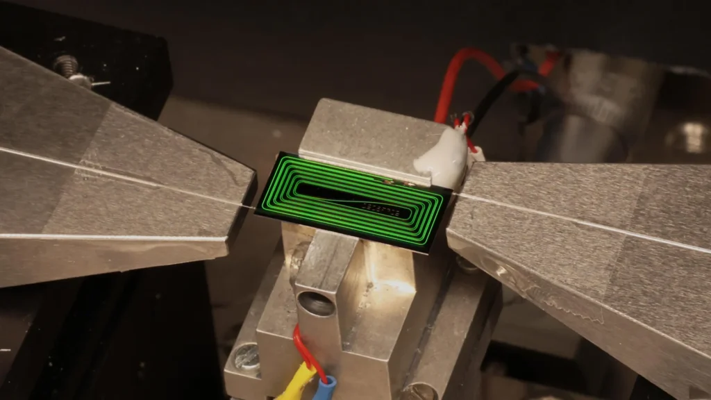
Now, researchers at EPFL, led by Professor Tobias J. Kippenberg, have announced a transformative breakthrough that promises to dramatically reshape the landscape of ultrafast laser technology. Their pioneering work, detailed in a recent publication in the prestigious journal Nature, describes the development of the first integrated ultrafast laser capable of matching, and in some aspects, exceeding the performance benchmarks of traditional tabletop femtosecond lasers. This groundbreaking device delivers pulse energies of 1.05 nanojoules (nJ) and achieves remarkably short pulse durations of just 147 femtoseconds (fs), all while residing on a compact photonic chip.
This achievement marks a critical inflection point, demonstrating that high-performance ultrafast laser functionality can be translated from sprawling optical setups to a microscopic scale. The significance of this miniaturization cannot be overstated, promising to liberate ultrafast laser technology from its traditional confines and make it accessible for a myriad of new applications that were previously unimaginable due to size and cost constraints.
Bringing Ultrafast Lasers to Photonic Chips: The Technological Leap
Photonic chips represent a paradigm shift in how light is manipulated and processed. Much like electronic chips guide and process electrical signals through etched pathways, photonic chips utilize microscopic structures called waveguides, fabricated onto a wafer, to direct and control light. These chips have already played a pivotal role in miniaturizing various optical technologies, particularly in telecommunications, where they have enabled the transition from bulky optical components to compact, high-performance devices.
The integration of ultrafast lasers onto such a platform has been an enduring challenge due to the complex interplay of light and matter required for stable, high-energy pulse generation. Traditional fiber lasers, while more compact than their free-space counterparts, still involve meters of optical fiber and discrete components, leading to systems that are orders of magnitude larger than a photonic chip. The EPFL team’s success in compressing this functionality onto a chip represents a monumental leap in integrated photonics.
Professor Kippenberg articulated the long-standing aspiration, stating, "For more than twenty years, a high-pulse-energy femtosecond laser on chip was widely regarded as a holy grail of integrated photonics." He further emphasized the elegance of their solution: "Our result shows that it is not only possible, but that it can be achieved with a surprisingly elegant architecture that the integrated-photonics community had overlooked." This underscores the novel approach taken by the team, moving beyond conventional designs that had previously proven difficult to integrate.
The Ingenious Architecture: Mamyshev Oscillator on a Chip
To accomplish this formidable feat, the researchers adopted a specific laser architecture known as the Mamyshev oscillator. This design, despite its potential, had historically received relatively little attention within the integrated photonics community. Its principles, however, proved exceptionally well-suited for the unique constraints and opportunities presented by a chip-scale platform.
The core of the Mamyshev oscillator system involves placing a nonlinear waveguide between two optical filters. Each of these filters is specifically engineered to transmit a distinct, different portion of the light spectrum. The operation hinges on a self-regulating mechanism: as an intense laser pulse propagates through the nonlinear waveguide, it undergoes a phenomenon known as spectral broadening. This effect causes the pulse to expand into a wider range of colors, or frequencies. A critical aspect is that only a specific, broadened portion of this light is then able to pass through both optical filters and continue circulating within the laser cavity, sustaining the oscillation.
Conversely, weaker light pulses behave differently. They do not possess sufficient intensity to induce the necessary degree of spectral broadening. As a result, they fail to expand into the spectral range required to pass through both filters. This effectively means that weaker light is blocked and removed from the laser cycle, ensuring that only robust, high-intensity pulses are allowed to circulate and grow. This self-cleaning mechanism is fundamental to the Mamyshev oscillator’s stability and its ability to generate high-quality ultrafast pulses.
The Advantages of the Overlooked Design
Zheru Qiu, a co-leading author of the paper, highlighted several key advantages of this particular design for integrated photonics. "This design is especially attractive because it does not require any component that is difficult to make on this erbium-doped silicon nitride chip," Qiu explained. The choice of materials, specifically erbium-doped silicon nitride, is crucial. Erbium is a rare-earth element commonly used as a gain medium in lasers, and its integration into a silicon nitride waveguide allows for efficient light amplification directly on the chip. Silicon nitride itself is a highly desirable material for integrated photonics due to its low optical loss and high nonlinearity, which are essential for the Mamyshev oscillator’s operation.
Beyond ease of fabrication, the Mamyshev oscillator offers another significant benefit that addresses a fundamental challenge in integrated photonics. Photonic chips, by their very nature, confine light within extremely small waveguides. This tight confinement leads to a strong interaction of light with itself, enhancing nonlinear optical effects. While these nonlinearities are essential for many chip-based devices, in many conventional laser architectures, they can also lead to instability and distortion of the laser pulses. The Mamyshev oscillator, however, exhibits a remarkable resilience to these issues. Its self-filtering mechanism intrinsically manages and utilizes these nonlinear effects to shape and stabilize the pulses, making it uniquely well-suited for integrated photonic devices where strong nonlinearities are inherent.
Unprecedented Miniaturization and Scalability
The physical scale of this achievement is truly remarkable. While the laser cavity itself measures 42 centimeters in length, the ingenious design allows it to be folded onto a photonic chip occupying roughly the area of a match head. This dramatic reduction in size renders the integrated laser significantly smaller than even conventional fiber-based ultrafast lasers, which themselves are considered compact compared to older tabletop systems.
This miniaturization is not merely a feat of engineering; it has profound implications for manufacturing and accessibility. Photonic chips can be manufactured at wafer scale, leveraging highly developed techniques similar to those employed for producing computer chips. This means that, in principle, more than 1,000 laser cavities could be fabricated simultaneously on a single wafer. This wafer-scale manufacturing advantage could usher in a new era of affordability for ultrafast lasers, drastically reducing their cost and making them accessible for a much broader range of applications.
"With kilowatt-level peak powers, the chip can drive demanding applications that have long depended on large, expensive laboratory lasers," Qiu noted. To put this in perspective, the reported pulse energy of 1.05 nJ delivered in 147 fs translates to a peak power of approximately 7.14 kilowatts (kW). Such high peak powers are crucial for applications requiring intense, short bursts of energy, such as nonlinear microscopy, material processing, and advanced spectroscopy. Achieving this power density from a match-head sized device fundamentally changes the economic and logistical landscape for these technologies.
Far-Reaching Implications Across Industries
The implications of this breakthrough extend across numerous scientific, industrial, and medical sectors. The ability to produce powerful, compact, and cost-effective ultrafast lasers on a chip promises to democratize a technology that was once the exclusive domain of well-funded laboratories and specialized industries.
Sensing and Spectroscopy: Miniaturized ultrafast lasers could revolutionize environmental monitoring. Portable devices could be developed for detecting pollutants in air and water with unprecedented sensitivity and speed, offering real-time data collection in the field rather than relying on lab-based analysis. In spectroscopy, the broad spectral output of femtosecond lasers is invaluable for identifying chemical compositions. Chip-scale versions could enable ubiquitous, handheld spectrometers for everything from food quality control to security screening.
Precision Measurement: The role of ultrafast lasers in precision measurement, particularly in the context of optical frequency combs, is already established. This new integrated platform could lead to highly compact and robust optical atomic clocks, which are essential for next-generation global positioning systems (GPS), ultra-secure communication networks, and fundamental physics research. Imagine GPS receivers with orders of magnitude higher accuracy, or quantum computing platforms benefiting from precise timing.
Industrial Applications: In manufacturing, the precision offered by ultrafast lasers for micro-machining, drilling, and surface structuring could become more widely available. Industries currently constrained by the cost and size of laser systems could integrate these capabilities directly into production lines, enabling more intricate designs and higher quality products at a lower cost. Identifying hidden defects in materials, a crucial aspect of quality control in aerospace and automotive industries, could also become a routine, on-site procedure with portable devices.
Medical Diagnostics and Treatment: The medical field stands to gain immensely. Portable and affordable devices could be developed for advanced medical diagnostics, such as non-invasive imaging techniques like optical coherence tomography (OCT) with enhanced resolution, directly at the point of care. This could lead to earlier disease detection, more accurate surgical guidance, and personalized treatments. The precision of femtosecond lasers in eye surgery (e.g., LASIK) could also become more accessible and potentially integrated into smaller, more versatile surgical platforms. Beyond surgery, their use in selective cell ablation or drug delivery mechanisms could open new avenues for targeted therapies.
Future Horizons: From Diagnostics to Navigation
The researchers believe that this technology could pave the way for a future where high-performance ultrafast lasers are as ubiquitous as microprocessors are today. The vision includes devices that can be deployed anywhere, from remote environmental monitoring stations to personal medical diagnostic kits, fundamentally altering how we interact with and understand the physical world.
The long-term impact on communications and navigation systems could be particularly transformative. Compact optical atomic clocks, enabled by these integrated lasers, could play vital roles in future quantum technologies, offering unparalleled synchronization and precision for a variety of applications, from distributed sensor networks to advanced cryptographic systems. The ability to produce these complex devices on a wafer scale promises to accelerate the pace of innovation across a multitude of disciplines, making high-end optical science a more accessible and integrated part of our technological future.
This groundbreaking work was the result of a collaborative effort involving researchers from the EPFL Institute of Electrical and Microengineering and Helmholtz-Zentrum Dresden-Rossendorf (HZDR), highlighting the international and interdisciplinary nature of cutting-edge scientific discovery. The integration of high-performance ultrafast lasers onto a chip is not merely an engineering triumph; it represents a significant step towards democratizing access to one of the most powerful tools in modern science, with implications that will resonate across industries and fundamentally enhance our technological capabilities for decades to come.