In a significant leap for the field of quantum photonics, researchers at the University of Technology Sydney (UTS) have successfully demonstrated a novel technique to manipulate tiny sources of quantum light. By physically twisting atomically thin layers of hexagonal boron nitride (hBN), the team has unlocked a high-precision "lever" for tuning quantum emitters, a breakthrough that addresses one of the primary hurdles in the transition of quantum technologies from the laboratory to real-world applications.
The study, led by Dr. Angus Gale and supervised by Professor Igor Aharonovich, focuses on the behavior of quantum emitters—microscopic sources capable of emitting single photons. These individual particles of light are the fundamental building blocks for a suite of emerging technologies, including quantum computing, ultra-secure communication networks, and highly sensitive biological sensors. Until now, the ability to precisely control the properties of these emitters, such as their color and wavelength, has been limited by the rigid nature of traditional semiconductor materials.
The Science of Hexagonal Boron Nitride and Twistronics
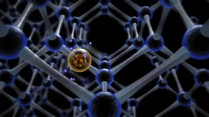
At the heart of this discovery is hexagonal boron nitride, a versatile material often referred to as "white graphene" due to its hexagonal lattice structure and two-dimensional nature. Unlike traditional three-dimensional crystals like diamond or silicon carbide, which are commonly used as hosts for quantum emitters, hBN is composed of layers held together by weak van der Waals forces.
This layered architecture allows for a phenomenon known as "twistronics." In the world of condensed matter physics, twistronics involves rotating layers of 2D materials relative to one another to fundamentally change their electronic and optical properties. While twistronics has been famously used to induce superconductivity in graphene, the UTS team is among the first to apply this principle to the control of quantum light sources embedded within the material.
Dr. Gale explained that the inherent flexibility of hBN provides a unique advantage. "We’re leveraging the fact that this material is layered. We can pick it up, stack it, and twist it. You can’t really do that with traditional materials where the atoms are locked in a three-dimensional lattice," he said. This "pick-up-and-place" method allows researchers to manipulate the material at the atomic scale, providing a level of tunability that was previously thought unattainable in solid-state systems.
Breakthrough Experimental Results
During the experimental phase, the UTS researchers observed that the act of twisting the hBN layers caused a dramatic shift in the light emitted by the defects within the crystal. These defects, which act as the quantum emitters, are essentially "missing" atoms or "substitute" atoms that trap electrons and release energy in the form of photons.
The most striking finding was the magnitude of the change. In traditional quantum systems, tuning the emission wavelength often requires extreme conditions, such as intense cryogenic cooling, massive pressure, or strong magnetic fields, and even then, the resulting shifts are often marginal. However, by using the twistable hBN platform, the team achieved a wavelength shift that was significantly larger than predicted by current theoretical models.
"Often when you control these systems, the amount of manipulation is very limited," Dr. Gale noted. "In this case, the shift was much larger than expected. Rather than trying to make hBN defects behave like a traditional solid-state host, we took advantage of hBN’s own strength: its thin, layered, twistable structure."
The researchers were able to demonstrate a repeatable process of lifting, rotating, and restacking the layers. This capability is crucial because it means the properties of the quantum emitter are not fixed during the fabrication process. Instead, they can be "tuned" dynamically, allowing scientists to reach the exact specifications required for a particular quantum operation.
The "Cheese Slice" Analogy and Material Innovation
To illustrate the difference between hBN and conventional materials, Dr. Gale utilized a culinary analogy. He compared traditional materials like diamond or silicon carbide to a solid block of cheese. "With a block of cheese, you can’t really get to the flavor in the middle without destroying the block," he explained. "But with slices, you can peel away layers, put them back together, and change how they interact."
This accessibility is the defining characteristic of 2D materials. Because every atom in an hBN layer is effectively on the surface, the environment surrounding a quantum emitter can be modified simply by changing what is placed next to it or how it is oriented. This makes hBN an ideal candidate for integrated quantum photonics, where multiple components must be precisely aligned and tuned to work in harmony.
Supporting Data and Technical Implications
The UTS study contributes vital data to the ongoing effort to standardize quantum light sources. One of the greatest challenges in quantum networking is "indistinguishability." For two photons to interfere with each other—a requirement for quantum gates in a light-based quantum computer—they must be identical in every way, including their frequency and phase.
In nature, quantum emitters are rarely identical; slight variations in the local environment of the crystal lattice cause them to emit light at slightly different frequencies. The "twist" method provides a mechanical solution to this problem. By adjusting the angle between layers, researchers can potentially "fine-tune" different emitters until their outputs match perfectly.
Furthermore, hBN emitters are known to operate at room temperature, a significant advantage over many other quantum systems that require liquid helium cooling to near absolute zero. The combination of room-temperature operation and mechanical tunability positions hBN as a frontrunner for the commercialization of quantum hardware.
Official Responses and Future Outlook
Professor Igor Aharonovich, a leading expert in nanophotonics and the supervising author of the research, emphasized that the ability to twist layered materials reveals entirely new physical behaviors. "You can take two layers that don’t do much on their own, put them together at a specific angle, and suddenly you have a completely different system," he said.
According to Aharonovich, the findings have far-reaching implications for several sectors:
- Cybersecurity: Quantum Key Distribution (QKD) relies on single photons to create unhackable communication lines. The ability to tune emitters ensures more reliable and efficient photon production for these networks.
- Healthcare: Quantum sensors can detect magnetic fields or chemical changes at the cellular level. Tunable emitters could lead to more sensitive diagnostic tools that can be calibrated for specific biological markers.
- Navigation and GPS: Improved quantum timing devices and accelerometers could lead to "quantum GPS" systems that do not rely on satellite signals, providing high-precision navigation in environments where satellites are blocked, such as underwater or in deep space.
"This gives us more control over the building blocks needed to get to the realization of quantum technologies," Aharonovich added.
Analysis of Broader Impact
The research at UTS arrives at a time when the global "quantum race" is intensifying. Governments and private entities are investing billions of dollars into quantum sovereignty. Australia, in particular, has identified quantum technology as a critical area for national interest, with the government launching a National Quantum Strategy to foster local innovation.
The work by Gale and Aharonovich highlights a shift in the research community from merely "discovering" quantum effects to "engineering" them. For decades, scientists were at the mercy of the natural properties of materials. The move toward "designer materials" through twistronics suggests that the next generation of technology will be defined by our ability to manipulate matter at the atomic level to meet specific functional requirements.
However, challenges remain. While the UTS team has proven the concept in a controlled laboratory setting, scaling this process to mass-produce thousands of perfectly twisted quantum chips remains a significant engineering hurdle. The "pick-up-and-place" method is currently a delicate process that requires high precision. Future research will likely focus on automating this technique and integrating it into existing semiconductor manufacturing workflows.
Conclusion
The demonstration of twist-controlled quantum emitters at the University of Technology Sydney represents a paradigm shift in how scientists approach light-matter interaction. By moving away from the "static" nature of traditional crystals and embracing the "dynamic" possibilities of layered 2D materials, the researchers have provided a vital tool for the quantum toolkit.
As Dr. Gale concluded, the work is a "step towards the realization of quantum technologies," moving the field closer to a future where quantum computers and secure networks are no longer theoretical constructs, but practical tools that solve some of the world’s most complex problems. The ability to "twist" the properties of light ensures that the path toward the quantum age is becoming increasingly precise and adaptable.