The global demand for electricity is accelerating at an unprecedented rate, driven largely by the expansion of digital infrastructure, the rise of artificial intelligence, and the proliferation of information and communications technology (ICT). Current estimates suggest that data centers and ICT networks already account for between 6 and 12 percent of the world’s total electricity consumption, a figure that is projected to climb as society becomes increasingly digitized. Amidst this rising energy crisis, a breakthrough from the Chalmers University of Technology in Sweden offers a promising pathway toward a new generation of ultra-efficient electronics. By developing a method to "sculpt" the surfaces upon which superconducting materials are grown, researchers have successfully enhanced the ability of these materials to function at higher temperatures and withstand intense magnetic fields—two of the most significant barriers to the commercialization of superconducting technology.
Superconductors represent a "holy grail" for materials science because they possess the unique ability to conduct electricity with zero resistance. Unlike conventional conductors like copper or aluminum, which lose energy in the form of heat due to the collision of electrons with the material’s atomic lattice, superconductors allow electrons to flow in synchronized pairs, known as Cooper pairs. In theory, replacing current silicon-based electronics and copper power grids with superconducting alternatives could improve energy efficiency by hundreds of times, virtually eliminating transmission losses and drastically reducing the cooling requirements for massive server farms. However, the transition from laboratory curiosity to industrial standard has been stalled for decades by the extreme environmental conditions these materials require to operate.
The Dual Barriers of Temperature and Magnetism
To understand the significance of the Chalmers breakthrough, one must first consider the inherent limitations of known superconducting materials. The first major hurdle is the "Critical Temperature" ($T_c$). For most of the 20th century, superconductivity was only achievable at temperatures near absolute zero (-273.15 degrees Celsius), necessitating the use of liquid helium, which is both scarce and expensive. While the discovery of high-temperature superconductors (HTS) in the 1980s—specifically the cuprate family—raised the operating threshold to around -200 degrees Celsius, this still requires specialized cryogenic cooling using liquid nitrogen. While more affordable than helium, nitrogen cooling remains a complex logistical and energy-intensive burden for consumer electronics.
The second hurdle is the "Critical Magnetic Field" ($H_c$). Superconductivity is a delicate state of matter. When exposed to a sufficiently strong magnetic field, the Cooper pairs that facilitate zero-resistance flow are torn apart, causing the material to revert to a resistive, "normal" state. This is a profound problem for practical applications, as many of the technologies that would benefit most from superconductivity—such as quantum computers, high-speed maglev trains, and advanced medical imaging—generate or operate within powerful magnetic environments.
For years, the scientific community has focused on chemical doping—altering the internal molecular structure of superconductors—to make them more robust. However, these chemical modifications are difficult to control and often result in brittle materials that lose their effectiveness when manufactured into the thin films required for modern microchips.
A Paradigm Shift in Material Engineering
The team at Chalmers University of Technology, led by Floriana Lombardi, Professor of Quantum Device Physics, decided to abandon the traditional focus on chemical composition in favor of "interfacial engineering." Instead of changing what the superconductor is made of, they changed the surface it sits on.
The researchers worked with a specific cuprate known as Yttrium Barium Copper Oxide (YBCO). This material is a high-temperature superconductor, but it is notoriously sensitive to its environment. In their experiment, the team produced an ultrathin layer of YBCO, measuring only a few nanometers in thickness—roughly one-millionth the width of a human hair. Because the film is so thin, its properties are heavily influenced by the "substrate," the underlying foundation upon which the film is grown.
"By sculpting the surface that the superconductor rests on, we were able to induce superconductivity at significantly higher temperatures than previously possible," explained Professor Lombardi. "We also found that the material remained superconducting even when exposed to strong magnetic fields."
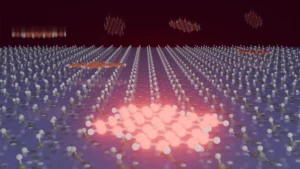
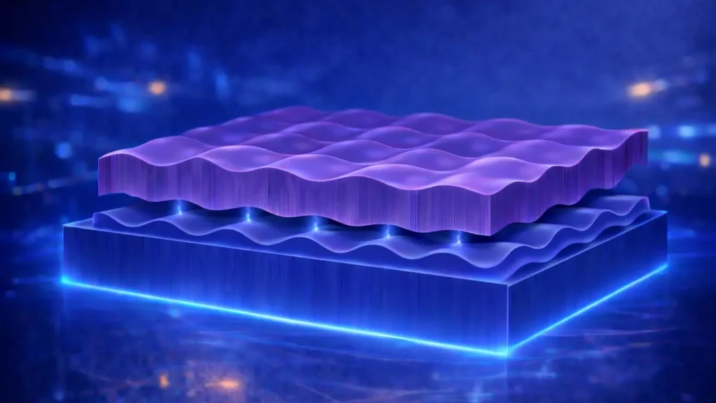
The process involved a sophisticated vacuum heat treatment of the substrate before the YBCO was applied. By heating the substrate in a controlled vacuum, the researchers caused the surface atoms to rearrange into an orderly, microscopic pattern of ridges and valleys, a process known as "nanofaceted" sculpting. This textured surface acted as a template, guiding the atoms of the superconducting YBCO film as they settled into place.
The Mechanics of Nanofaceted Substrates
When the superconducting film grows on this sculpted surface, the ridges and valleys create a specific electronic environment at the interface where the two materials meet. The atoms in the YBCO layer align themselves according to the substrate’s geometry, which in turn influences the behavior of the electrons within the film.
Eric Wahlberg, a researcher at the RISE Research Institutes of Sweden and a key contributor to the study, noted that the atomic arrangement of the substrate "guides" the settlement of the superconducting layer. This guidance creates a "preferential direction" for electron movement. In the interfacial region, this directional bias helps stabilize the formation of Cooper pairs, making them more resilient to thermal fluctuations (heat) and external magnetic interference.
The results, published in the journal Nature Communications, demonstrate that these nanofaceted surfaces allow the YBCO films to maintain their superconducting state under conditions that would typically cause them to fail. By strengthening the "pinning" of magnetic flux lines—a phenomenon where the magnetic field is essentially trapped in small pockets so it cannot disrupt the overall flow of electricity—the sculpted substrate allows the superconductor to remain functional in high-field environments.
Chronology of Superconductivity and the Path to the Present
To appreciate the context of this discovery, it is helpful to look at the timeline of superconductivity research:
- 1911: Heike Kamerlingh Onnes discovers superconductivity in solid mercury cooled to 4.2 Kelvin (-269°C).
- 1957: The BCS Theory (Bardeen, Cooper, and Schrieffer) explains the mechanism of superconductivity in metals.
- 1986: Georg Bednorz and K. Alex Müller discover high-temperature superconductivity in a lanthanum-based cuprate, shattering previous temperature limits and winning the Nobel Prize.
- 1987-1990s: Researchers identify YBCO and other cuprates that can operate at the temperature of liquid nitrogen (-196°C).
- 2010s: Focus shifts toward "room-temperature" superconductivity, with controversial and often retracted claims involving high-pressure hydrogen compounds.
- 2024: The Chalmers team introduces substrate sculpting as a viable alternative to chemical doping for enhancing the stability of thin-film superconductors.
The Chalmers discovery marks a shift from searching for new materials to optimizing existing ones through structural design. This is particularly relevant for the electronics industry, which relies heavily on thin-film deposition techniques similar to those used in the study.
Analysis of Implications: Energy, Quantum, and Beyond
The implications of this research extend far beyond the laboratory. If superconductivity can be stabilized at higher temperatures and in stronger magnetic fields, the "Great Energy Transition" could be significantly accelerated.
1. Data Centers and the AI Boom:
Modern data centers waste nearly 40% of their electricity on cooling systems designed to dissipate the heat generated by traditional silicon processors. Superconducting logic gates, which operate with zero resistance, produce virtually no heat. By utilizing the Chalmers method to create more robust superconducting circuits, the energy footprint of global AI processing could be slashed by an order of magnitude.
2. The Power Grid:
Current electrical grids lose approximately 5% to 10% of their energy during transmission and distribution. Superconducting cables, stabilized by nanofaceted substrates, could transport electricity from offshore wind farms or desert solar arrays to cities with zero loss, regardless of the distance.
3. Quantum Computing:
Quantum bits (qubits) are incredibly sensitive to environmental noise. Many quantum architectures rely on superconducting circuits that must be shielded from even the smallest magnetic fluctuations. The ability to "engineer" a substrate that inherently resists magnetic interference could lead to more stable, scalable quantum computers that do not require the massive, multi-million dollar dilution refrigerators currently in use.
4. Medical and Scientific Imaging:
MRI machines and particle accelerators require massive superconducting magnets. Currently, these machines are bulky and expensive because of the immense cooling systems needed to keep the magnets functional. Higher-temperature, field-resistant superconductors could lead to portable MRI machines and more affordable diagnostic tools.
Global Collaboration and Peer Reaction
The study was a massive international effort, reflecting the global importance of the findings. Researchers from the RISE Research Institutes of Sweden, the University of Venice, the Birla Institute of Technology and Science in India, and several institutions in France and Germany contributed to the work. This collaborative approach suggests a high level of peer validation for the "substrate sculpting" theory.
While the broader scientific community has reacted with cautious optimism, experts note that the next challenge will be scaling this process. Growing a few nanometers of YBCO on a specialized substrate in a vacuum is a precise laboratory task; reproducing this at the scale of industrial wafer fabrication will require further engineering. However, because the technique relies on modifying the substrate—a process that can be integrated into existing semiconductor manufacturing pipelines—it is viewed as more "industry-ready" than many other theoretical superconductivity breakthroughs.
"This shows that very small changes at the nanoscale can have decisive effects," Professor Lombardi concluded. "We are now showing how superconductivity can be enhanced by sculpting the substrate, potentially unlocking the full potential of these materials for the future of electronics."
Conclusion
The work at Chalmers University of Technology provides a new design principle for the next century of materials science. By shifting the focus from the internal chemistry of superconductors to the physical morphology of their environment, the research team has bypassed long-standing technical hurdles. As the world grapples with the dual challenges of increasing computational needs and the urgent necessity for energy conservation, the ability to "sculpt" the path for lossless electricity may prove to be one of the most critical technological pivots of the decade. The study, "Boosting superconductivity in ultrathin YBa2Cu3O7−δ films via nanofaceted substrates," now serves as a blueprint for a future where electronics are not only faster and more powerful but fundamentally more sustainable.