The successful integration of an air-stable, monolayer superconductor into a functional microwave circuit marks a transformative milestone in the field of quantum materials and hardware engineering. Researchers at the Massachusetts Institute of Technology (MIT), in collaboration with several international institutions, have pioneered a fabrication process that preserves the delicate properties of ultrathin superconductors while enabling their production at a scale suitable for industrial application. By utilizing a novel growth technique that shields the material from the moment of its creation, the team has overcome a decade-long hurdle in materials science: the rapid degradation of two-dimensional (2D) superconductors when exposed to oxygen and moisture.
The research, recently published in the journal Nature, demonstrates that these atomic-scale materials can maintain their superconducting properties—conducting electricity with zero resistance—while exhibiting exceptionally high kinetic inductance. This property is a critical resource for the development of next-generation quantum devices, including miniaturized qubits, ultrasensitive detectors for cosmological observation, and high-efficiency communication hardware.
The Engineering Challenge of Niobium Diselenide
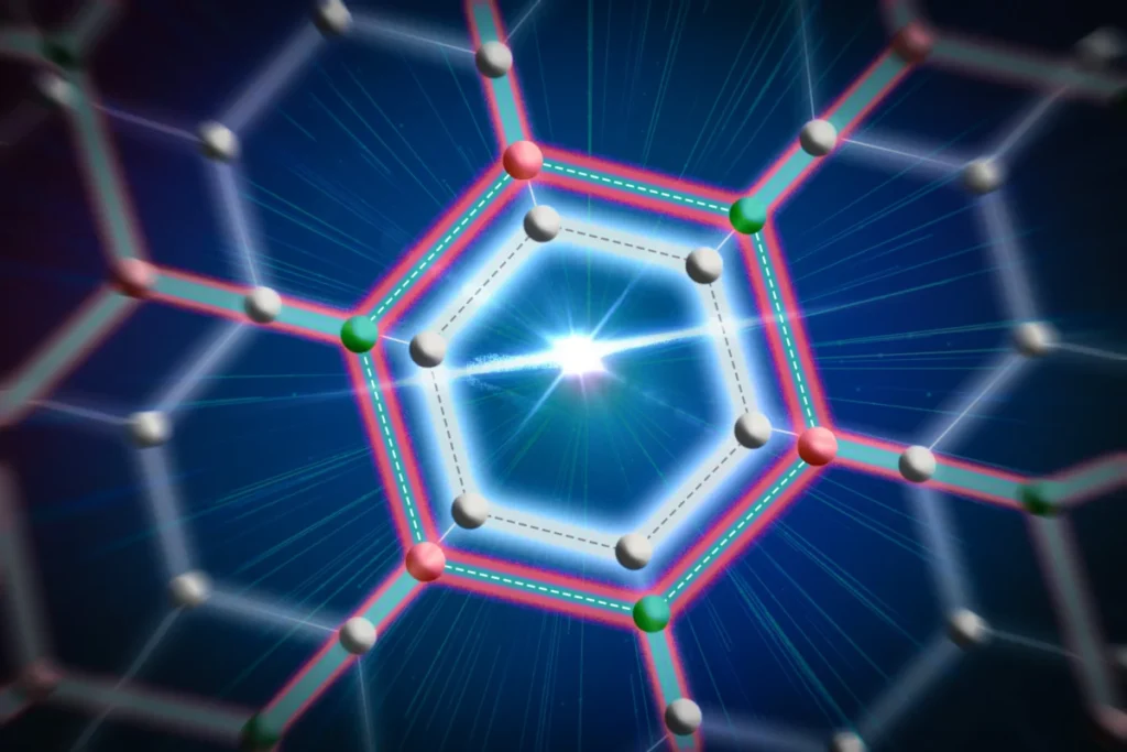
At the heart of this breakthrough is niobium diselenide ($NbSe_2$), a member of the transition metal dichalcogenide (TMD) family. In its monolayer form, $NbSe_2$ consists of a single layer of niobium atoms sandwiched between two layers of selenium atoms. Despite being only about one nanometer thick—thousands of times thinner than a human hair—this material possesses extraordinary electronic properties.
The primary appeal of monolayer $NbSe_2$ lies in its high kinetic inductance. In the context of superconducting circuits, inductance is the property that allows a material to store energy in a magnetic field or through the inertia of charge carriers. Kinetic inductance, specifically, arises from the mass of the superconducting electrons (Cooper pairs) as they move through the lattice. Because $NbSe_2$ is so thin and its charge carrier density is relatively low compared to bulk metals, it exhibits a kinetic inductance far higher than that of traditional superconducting films like aluminum or thick niobium.
For decades, the standard method for achieving high inductance in quantum circuits has been to string together long arrays of Josephson junctions—complex electronic components that act as non-linear inductors. While effective, these arrays are physically large, prone to noise, and difficult to manufacture with perfect uniformity. The ability to replace a bulky array of hundreds of junctions with a single, microscopic strip of $NbSe_2$ could drastically reduce the footprint of quantum processors, paving the way for the "scaling up" of quantum computers from dozens of qubits to thousands or millions.
However, $NbSe_2$ is notoriously "air-sensitive." Once removed from the ultra-high vacuum or inert gas environments where it is synthesized, it begins to oxidize within seconds. This oxidation destroys the superconducting state, turning the material into a non-functional insulator. Until now, researchers were forced to use "exfoliation"—the mechanical peeling of small flakes from a larger crystal using adhesive tape—to study the material. This "Scotch-tape method" produces tiny, irregular samples that are impossible to integrate into large-scale manufacturing processes.
A Novel Growth Strategy: Mind the Gap
The MIT-led team, spearheaded by co-lead authors Xudong Sheldon Zheng, Sameia Zaman, and Kenan Zhang, reimagined the synthesis process to solve the oxidation problem at its source. Traditionally, scientists grow 2D materials by depositing chemical precursors onto a silicon dioxide ($SiO_2$) substrate and then attempt to "cap" the material with a protective layer like graphene or hexagonal boron nitride (hBN) after the growth is complete. The fatal flaw in this approach is the "transfer gap"—the brief window of time where the material is exposed to the environment before the cap is applied.
The researchers inverted this logic. Instead of capping the superconductor after growth, they placed a layer of graphene onto the silicon dioxide substrate first. Through a process of careful thermal tuning and chemical vapor deposition, they introduced the precursors into the system. They discovered that the precursors could migrate into the "Van der Waals gap"—the infinitesimal space (less than one nanometer) between the graphene and the $SiO_2$ substrate.
"It took a long time for us to understand how the growth could happen underneath the graphene," explains Xudong Sheldon Zheng. "The silicon dioxide substrate helps trap the precursors long enough for the crystal to begin forming, while the graphene layer allows them to move around easily and spread into a continuous monolayer."
This "interfacial growth" technique ensures that the $NbSe_2$ is never exposed to air. From the moment the atoms arrange themselves into a crystal lattice, they are hermetically sealed between the graphene cap and the silicon substrate. This allowed the team to produce smooth, uniform layers of the superconductor over areas larger than one inch—a "wafer-scale" achievement that transitions the material from a laboratory curiosity to a viable industrial component.
Chronology of Development and Experimental Validation
The journey toward this breakthrough involved several years of iterative testing and interdisciplinary collaboration. The project built upon earlier work at MIT’s Research Laboratory of Electronics (RLE) regarding the properties of TMDs and the development of "oxidation-free transfer" techniques.
- Phase I: Discovery of High Kinetic Inductance (2021-2023): Members of the research team initially identified that thin-film niobium diselenide possessed the requisite inductance values to compete with Josephson junction arrays. This provided the theoretical motivation to find a way to scale the material.
- Phase II: Interfacial Growth Refinement: The team experimented with various "capping" materials, eventually settling on graphene due to its high thermal stability and the specific way it adheres to $SiO_2$, creating a perfectly sized pocket for $NbSe_2$ growth.
- Phase III: The Transfer and Etching Challenge: Even with a protected material, the team had to figure out how to connect it to the rest of a circuit. Sameia Zaman and the team developed a vacuum-etching process to expose only the side walls of the $NbSe_2$ layer, allowing for "edge contacts" with conventional metal electrodes.
- Phase IV: Microwave Circuit Integration: The final validation involved placing the graphene-encapsulated $NbSe_2$ into a superconducting microwave resonator. Testing at cryogenic temperatures confirmed that the material not only survived the fabrication process but also performed with the high quality-factor required for quantum operations.
The resulting paper, published in Nature, features a diverse roster of experts, including corresponding authors William D. Oliver (a leader in superconducting qubits), Jing Kong (a pioneer in 2D material synthesis), and Joel I-j. Wang of NYU. The collaboration extended to Rice University, Yale University, and Pohang University in South Korea, reflecting the global interest in 2D quantum materials.
Technical Analysis of Quantum Implications
The implications of this research extend far beyond simple miniaturization. In the field of quantum computing, the "size" of a circuit is often a limiting factor for coherence. Larger circuits are more susceptible to picking up stray electromagnetic noise from the environment, which leads to "decoherence"—the loss of the quantum state. By shrinking the inductive elements of a qubit using monolayer $NbSe_2$, engineers can create "tighter" circuits that are potentially more robust against external interference.
Furthermore, the high kinetic inductance of $NbSe_2$ makes it an ideal candidate for Kinetic Inductance Detectors (KIDs). These are used in experimental cosmology to detect faint signals from the Cosmic Microwave Background (CMB) or in deep-space communications. A KID works by measuring how incoming photons break Cooper pairs in a superconductor, which changes the material’s inductance and shifts the resonant frequency of the circuit. Because $NbSe_2$ is so thin, it is incredibly sensitive to even the smallest energy inputs, potentially allowing for detectors that can "see" deeper into the early universe or handle higher data rates in quantum telecommunications.
Broader Impact and Future Directions
The MIT team has emphasized that this growth strategy is not a "one-off" success for niobium diselenide. The method of growing materials in the Van der Waals gap between a substrate and a protective cap can likely be extended to an entire family of 2D materials. This includes other superconductors, semiconductors, and even topological insulators that are otherwise too unstable to be used in practical engineering.
"We’ve taken a very good step toward exploring both the physics and the application side of this thin, monolayer superconductor," says Sameia Zaman. "There are a lot of directions we can go in the future."
The research was supported by a wide array of high-level funding agencies, including the U.S. Army Research Office, the National Science Foundation (NSF), and the Department of Energy (DOE). This broad support underscores the strategic importance of superconducting materials for both national security (in the form of quantum-resistant cryptography) and fundamental scientific discovery.
As the industry moves toward the "Post-NISQ" (Noisy Intermediate-Scale Quantum) era, the focus is shifting from simply making qubits work to making them manufacturable, reliable, and compact. The ability to grow air-stable, high-performance superconductors at the wafer scale suggests that the transition from laboratory prototypes to commercial quantum hardware may be closer than previously anticipated. The MIT team’s work provides a blueprint for a new generation of "flat" quantum electronics, where the thickness of the material is no longer a limitation, but rather its greatest strength.