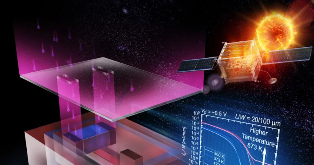
Engineers and scientists worldwide are continually pushing the boundaries of material science and semiconductor technology, seeking devices capable of operating under increasingly demanding conditions. A recent announcement from Kyoto University marks a significant stride in this endeavor, with a team of researchers successfully demonstrating a silicon carbide (SiC) junction field-effect transistor (JFET) that can function reliably at temperatures up to an astonishing 600°C. This breakthrough, utilizing standard ion implantation processes, holds profound implications for a myriad of applications ranging from deep space exploration to industrial process control and advanced propulsion systems.
The Quest for Extreme-Temperature Electronics
The relentless march of technological progress demands electronics that are not only faster and more powerful but also more resilient. Conventional silicon-based semiconductors, the backbone of modern electronics, begin to falter at temperatures exceeding 200-250°C. Beyond this threshold, silicon’s intrinsic carrier concentration rises dramatically, leading to increased leakage currents and loss of device control. This limitation has historically forced engineers to either relocate sensitive electronics away from heat sources, employ bulky and complex cooling systems, or significantly compromise on operational lifespan.
For decades, the scientific community has explored alternative semiconductor materials with wider bandgaps than silicon. A wider bandgap means more energy is required to excite electrons into the conduction band, leading to lower intrinsic carrier concentrations and better performance at elevated temperatures. Silicon Carbide (SiC) has emerged as a frontrunner among these "wide bandgap" semiconductors. Known for its robust physical and electronic properties, SiC boasts a bandgap approximately three times wider than silicon, superior thermal conductivity, and a much higher breakdown electric field. These characteristics have already made SiC a staple in power electronics, enabling more efficient power conversion in electric vehicles, solar inverters, and industrial motor drives. However, creating complex logic circuits from SiC that can withstand extreme temperatures has remained a formidable challenge.
Kyoto University’s Innovative Approach: Standard Manufacturing for Extreme Performance
The team at Kyoto University, led by Professor Tatsuya Kaneko, focused on developing a SiC JFET that could not only operate at unprecedented temperatures but also leverage manufacturing processes compatible with existing semiconductor fabrication infrastructure. This latter point is crucial for the eventual commercial viability and widespread adoption of such technology.
One of the primary hurdles in SiC device fabrication, particularly for achieving precise electrical characteristics, is the process of doping. Doping involves intentionally introducing impurity atoms (dopants) into the semiconductor material to alter its electrical conductivity. Ion implantation is a standard method for this, where ions of the dopant element are accelerated and embedded into the semiconductor substrate. While precise, ion implantation can suffer from a phenomenon known as "dopant channeling." In crystalline materials like SiC, if ions enter along specific crystallographic directions, they can penetrate deeper than intended, leading to an imprecise doping profile and inconsistent electrical properties, such as variations in the threshold voltage (the voltage required to turn the transistor on).
To counteract dopant channeling and gain superior control over the transistor’s electrical characteristics, the Kyoto researchers devised a novel "bottom-gate" structure for their SiC JFET. In a conventional JFET, the gate typically controls the channel from the top. By moving the gate to the bottom, the researchers found they could more effectively manage the current flow and mitigate the effects of dopant channeling. This architectural innovation significantly improved the predictability and consistency of the device. At 400°C, the difference between the designed and measured threshold voltage was dramatically reduced from over 2 V to less than 0.1 V, demonstrating an unprecedented level of control and precision for high-temperature operation.
Another critical challenge at extreme temperatures is electrical isolation. While SiC provides excellent insulation at room temperature, its insulating properties degrade as temperatures climb, leading to unwanted leakage currents through the substrate. To address this, the Kyoto team implemented a "double-well isolation structure." This design essentially places each transistor within its own pn junction, creating an electrical barrier that prevents current from straying through the substrate. This ingenious solution effectively isolates individual transistors, ensuring that current flows only through the intended paths and reportedly pushing the remaining leakage current close to the theoretical limit imposed by SiC itself.
A Step Beyond Previous High-Temperature Achievements
The significance of Kyoto University’s achievement is further underscored by its manufacturing methodology. Prior advancements in extreme-temperature SiC electronics, including systems developed by NASA that have operated above 500°C for short durations, often relied on specialized, non-standard manufacturing techniques. These bespoke processes, while effective for research prototypes, can be costly, complex, and difficult to scale for mass production. By utilizing standard ion implantation—a technique already widely employed in semiconductor fabs—the Kyoto University design offers a more direct pathway to integration with existing manufacturing processes, potentially accelerating its transition from laboratory to industry. This compatibility greatly enhances the technology’s appeal and its potential for broader adoption.
Remaining Challenges and Future Outlook

Despite this monumental achievement, several challenges remain before these 600°C SiC transistors can become widely deployed. One immediate limitation of the current device is its "normally-on" characteristic. A normally-on transistor conducts current even without a gate voltage applied, meaning it consumes standby power. For efficient complementary logic circuits, which are the foundation of most modern digital electronics, "normally-off" devices are essential. Normally-off transistors require a gate voltage to turn on, thus conserving power when idle. The Kyoto researchers have previously demonstrated complementary SiC JFET logic operating at 350°C and are now focused on adapting their new structure to develop normally-off devices, which will be critical for low-power, high-density logic applications at extreme temperatures.
Beyond the transistor itself, the broader electronic system presents considerable hurdles. A transistor, however robust, is only one component. For an entire electronic system to function reliably at 600°C, every other element—from interconnects (wires), passive components (resistors, capacitors), and packaging materials to circuit boards and sensors—must also be capable of withstanding such conditions for extended periods. Long-term reliability, including thermal cycling endurance, chemical stability, and mechanical integrity, remains a significant area of ongoing research. Materials for high-temperature interconnects, such as refractory metals like tungsten or platinum, and advanced ceramic packaging solutions are critical for transforming these individual transistors into functional, reliable electronic systems.
Transformative Applications: Where 600°C Electronics Will Thrive
The ability to operate electronics at 600°C opens up a vast array of application spaces that were previously inaccessible or required complex, often impractical, engineering workarounds.
Aerospace and Propulsion Systems: Gas turbines and jet engines are prime examples. The core of these engines operates at extreme temperatures, often exceeding 1000°C. Current sensors and control electronics are typically located in cooler sections, requiring long wiring harnesses that add weight, complexity, and introduce signal degradation. High-temperature SiC electronics could enable sensors and processing units to be placed directly within the engine’s hot section, closer to the point of measurement. This proximity would allow for more accurate real-time monitoring of critical parameters like temperature, pressure, and combustion efficiency, leading to optimized performance, improved fuel economy, enhanced safety, and predictive maintenance capabilities. Shorter interconnections also reduce electromagnetic interference, improving signal integrity.
Industrial Process Control: Furnaces, kilns, chemical reactors, and metal processing systems operate at intensely high temperatures. Integrating electronics directly into these environments would revolutionize process control. Imagine sensors that can monitor the exact chemical composition inside a reaction chamber or the precise temperature distribution within a glass furnace without needing to penetrate thick, insulated walls with cumbersome probes. Such in-situ monitoring would lead to tighter process control, higher product quality, reduced waste, and more efficient energy utilization. The elimination of extensive cooling infrastructure around sensitive components would also simplify system design and reduce operational costs.
Deep Space Exploration: The Venus Frontier: Perhaps one of the most captivating applications lies in space exploration, particularly for missions to Venus. With a crushing atmospheric pressure 92 times that of Earth and a searing surface temperature of approximately 465°C, Venus is an inferno where conventional silicon electronics quickly perish. The Soviet Venera landers and NASA’s Magellan mission provided invaluable data, but their surface operational lifespans were measured in mere minutes or hours, primarily due to the extreme heat. A transistor capable of operating at 600°C could enable future Venusian landers and rovers to perform sophisticated sensing, data processing, and even robotic manipulation directly within the planet’s hostile environment for weeks or months. This would allow for unprecedented scientific discovery, including detailed atmospheric and geological analysis, and a deeper understanding of planetary evolution.
Energy Sector: Nuclear and Geothermal Systems: In nuclear power plants, sensors are crucial for monitoring reactor core conditions, safety parameters, and waste storage. Operating close to intense radiation and heat sources, these sensors require extreme resilience. Similarly, geothermal energy systems involve drilling into Earth’s crust to tap into superheated reservoirs. Electronics capable of withstanding these high temperatures could enable more effective resource mapping, drilling optimization, and long-term monitoring of geothermal wells, improving the efficiency and safety of these sustainable energy sources.
Reduction in Cooling Infrastructure: A broader systemic advantage of high-temperature electronics is the potential to significantly reduce or even eliminate the need for active cooling systems. Cooling systems, whether liquid-based or air-based, add substantial weight, consume power, occupy valuable space, and introduce points of failure, increasing overall system complexity and cost. By allowing electronics to simply tolerate the ambient temperature, engineers can design lighter, more compact, more reliable, and more energy-efficient systems. This simplification extends beyond the electronics themselves, impacting the overall thermal management strategy of entire platforms.
Conclusion: A Glimpse into the Future of Resilient Electronics
The research from Kyoto University represents a pivotal moment in the development of extreme-environment electronics. By demonstrating a 600°C SiC JFET using fabrication techniques that are compatible with existing industry standards, the team has significantly lowered the barrier to entry for this transformative technology. While the journey from laboratory prototype to commercial product involves overcoming significant hurdles related to normally-off device development, packaging, and long-term reliability, the fundamental breakthrough is undeniable.
As the demand for electronics in harsh and previously inaccessible environments continues to grow—from the depths of space to the heart of jet engines and industrial furnaces—the innovations in wide bandgap semiconductors like SiC will be paramount. Kyoto University’s achievement brings us closer to a future where electronics are not merely protected from extreme conditions but are designed to thrive within them, unlocking new frontiers of scientific discovery, industrial efficiency, and technological capability. The ripple effects of this research are poised to reshape numerous industries and expand the very definition of where and how electronic systems can operate.