The persistent challenge of overheating, a phenomenon familiar to any laptop user, represents one of the most significant barriers to the advancement of global computing infrastructure, from localized mobile devices to the massive data centers that underpin the modern internet. As semiconductor manufacturers continue to push the boundaries of Moore’s Law by packing billions of transistors into increasingly compact, multilayered architectures, the management of thermal energy has transitioned from a secondary engineering concern to a primary existential threat for the industry. While computer chips have become exponentially more powerful, the physics of heat dissipation has struggled to keep pace, leading to performance throttling, hardware failure, and massive energy inefficiencies.
In a landmark study published in Nature Communications, a multidisciplinary team of researchers from the Massachusetts Institute of Technology (MIT), in collaboration with Argonne National Laboratory and the University of Texas at Austin, has demonstrated a breakthrough methodology for observing heat transport at the microscopic level. By combining high-energy X-rays with ultrafast laser pulses, the researchers have successfully mapped how heat moves through complex, multilayered electronic materials with unprecedented precision. This technique allows for the identification of specific, nanoscale defects that obstruct thermal flow—defects that were previously invisible to conventional diagnostic tools.
The Thermal Wall: A Growing Crisis in Semiconductor Design
The semiconductor industry is currently facing what experts call the "thermal wall." For decades, the primary goal of chip design was to increase clock speeds and transistor density. However, as components shrink toward the atomic scale, the heat generated per square millimeter has skyrocketed. In high-performance environments, such as those housing AI-training clusters or cloud servers, cooling costs can account for up to 40% of total operational expenses.
The fundamental issue lies in the materials themselves. Modern electronics are rarely made of a single substance; they are "sandwiches" of various materials including silicon, gallium nitride, metals, and insulators. Each interface between these layers acts as a potential barrier to heat. If heat cannot escape the chip efficiently, "hotspots" form. These localized areas of extreme temperature can degrade the material over time, leading to the catastrophic failure of the device.
To engineer better chips, scientists must understand exactly how heat—carried by atomic vibrations known as phonons—traverses these layers. Until now, the industry lacked a non-destructive way to look deep inside a functioning, multilayered device to see this process in real-time.
Limitations of Traditional Thermal Metrology
Before this breakthrough, researchers relied on several established methods to measure thermal conductivity, each with significant drawbacks. One of the most common techniques is Time-Domain Thermoreflectance (TDTR). While effective for measuring the surface temperature of a material, TDTR uses visible light (optics), which cannot penetrate the opaque metallic or semiconducting layers found in real-world devices. Consequently, TDTR provides an "average" thermal reading of the entire stack rather than a layer-by-layer analysis.
Other methods, such as infrared thermography, suffer from low spatial resolution. While an infrared camera can show that a chip is hot, it cannot zoom in far enough to see why a specific micron-scale connection is failing. Furthermore, the frame rates of these cameras are far too slow to capture the ultrafast dynamics of heat propagation, which occurs on the scale of picoseconds (trillionths of a second).
"When doing these diagnoses using traditional techniques, they couldn’t get down to the micro- or nanometer scale," explained Mingda Li, an associate professor of nuclear science and engineering at MIT and co-corresponding author of the study. "But eventually, they’d like to go beyond that to study the heat carriers and understand exactly what causes failure, in order to avoid local hotspots and design better devices."
A New Diagnostic Frontier: X-rays and Laser Pulses
The MIT-led team addressed these limitations by pivoting from visible light to X-rays. Unlike optical lasers, X-rays have the energy required to penetrate multiple layers of a device without damaging the structure. The researchers utilized the Advanced Photon Source at Argonne National Laboratory, which provides one of the brightest X-ray sources in the world.
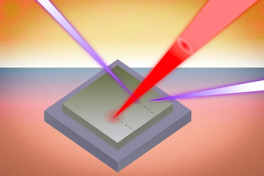
The experimental setup involves a "pump-probe" configuration. First, an ultrafast laser pulse (the "pump") hits the material, delivering a localized burst of heat. Immediately following the heat pulse, a series of X-ray pulses (the "probe") scans the material. As the heat moves through the various layers, it causes the atomic lattice of the material to expand slightly—a phenomenon known as thermal strain.
By measuring the diffraction of the X-rays, the researchers can calculate this strain at the atomic level across different depths and positions. This allows them to create a real-time, three-dimensional movie of heat dissipation. This approach provides a clear view of how heat propagates across the interfaces where different materials meet, allowing researchers to resolve what happens on one specific layer versus another.
Case Study: The Hidden Impact of Micron-Scale Defects
To test the efficacy of their new method, the researchers applied it to a promising semiconductor architecture: a layer of gallium nitride (GaN) grown on top of a silicon substrate. GaN is a "wide-bandgap" semiconductor that is increasingly used in power electronics, 5G base stations, and electric vehicle inverters because it can handle much higher voltages and temperatures than traditional silicon.
However, the process of growing GaN on silicon often introduces "wrinkle defects"—tiny structural imperfections that occur during the manufacturing process. While these defects have been known to exist, their specific impact on thermal performance remained a matter of theory and simulation rather than direct observation.
The MIT team’s measurements revealed a startling reality. A single micron-scale wrinkle defect caused a fourfold (75%) reduction in the material’s ability to transfer heat at that specific spot. Furthermore, the researchers discovered that the defect introduced thermal anisotropy—meaning heat moved more easily in one direction than the other, leading to uneven spreading and the formation of dangerous hotspots.
"When people model heat dissipation, they model perfect crystals without defects," Li noted. "But these types of large wrinkle defects are very common. People never even knew how much heat is blocked by these wrinkles. Those are things we can now directly observe with this technique."
Chronology of the Research and Industry Collaboration
The development of this technique follows a decade of intensifying research into thermal management.
- 2015–2018: Industry leaders begin sounding the alarm on the "thermal limit" of silicon-based air-cooled systems, prompting a surge in research into liquid cooling and new materials like GaN.
- 2020: The MIT team begins conceptualizing a method to utilize high-brightness X-rays for thermal mapping, seeking to move beyond the surface-level limitations of optical TDTR.
- 2022–2023: Experiments are conducted at the Argonne National Laboratory. The team successfully synchronizes ultrafast laser heating with X-ray diffraction measurements.
- 2024: The findings are published in Nature Communications, detailing the quantitative impact of defects on GaN-on-Silicon architectures.
The significance of the work has already garnered attention from the private sector. A leading semiconductor industry consortium has reportedly reached out to the MIT team to collaborate on applying this measurement technique to commercial chip designs. This suggests a rapid transition from academic proof-of-concept to industrial application.
Broader Implications for AI, Wearables, and Clean Energy
The ability to map heat flow at the nanoscale has profound implications for several high-growth sectors:
Artificial Intelligence and Data Centers: Modern AI chips, such as those produced by NVIDIA and AMD, generate massive amounts of heat. As these chips move toward "chiplet" designs and 3D-stacked memory (HBM), the number of material interfaces increases. This new X-ray technique could allow engineers to verify the thermal integrity of these stacks before they go into mass production.
Wearable Technology: In devices like smartwatches or medical sensors, there is no room for cooling fans. Thermal management must be handled entirely through material design. By understanding how heat moves through flexible electronics, companies can create more powerful devices that remain comfortable and safe against the skin.
Clean Energy Systems: Power inverters for solar grids and electric vehicles rely on GaN and Silicon Carbide (SiC) to convert energy efficiently. Overheating in these systems leads to energy loss and shortened lifespans. MIT’s technique offers a way to optimize the "packaging" of these power modules to ensure maximum longevity.
Conclusion: Designing the Next Generation of "Thermal-Aware" Electronics
The work led by Mingda Li, Jeehwan Kim, and their colleagues marks a shift in how the electronics industry approaches hardware failure. Instead of reacting to overheating after a device is built, engineers can now use direct experimental data to design "thermal-aware" architectures.
"This will enable better thermal design of electronic systems," said Jeehwan Kim, an associate professor at MIT and co-corresponding author. "Even with the same type of materials, the geometry and how the materials are laid out is quite complicated. This approach shows us how those differences impact thermal flow by providing direct experimental measurements."
As the world demands more computational power for everything from autonomous driving to generative AI, the bottleneck is no longer just how fast electrons can move, but how quickly the resulting heat can be removed. With this new X-ray diagnostic tool, the path toward cooler, more efficient, and more powerful electronics has become significantly clearer.
The research was supported by a coalition of institutions, including the U.S. Department of Energy, the U.S. National Science Foundation, and the MIT School of Engineering, reflecting the high level of national priority placed on maintaining semiconductor leadership through advanced thermal management.