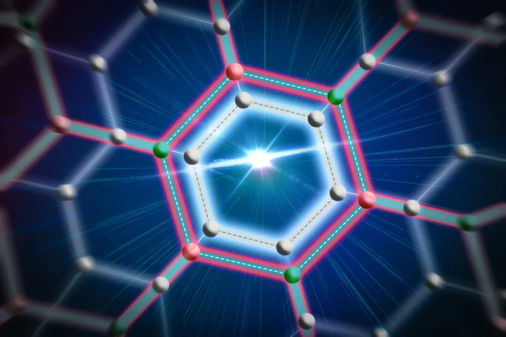
In a significant stride toward the miniaturization and stabilization of quantum hardware, a multidisciplinary team of researchers at the Massachusetts Institute of Technology (MIT) has pioneered a revolutionary fabrication technique for ultra-thin, air-stable superconductors. The breakthrough, detailed in a study published today in the journal Nature, addresses a long-standing bottleneck in materials science: the extreme fragility and rapid degradation of monolayer superconductors when exposed to ambient environments. By successfully integrating these materials into superconducting microwave circuits, the team has demonstrated a path toward scalable, high-performance quantum devices that could redefine the landscape of quantum computing, telecommunications, and deep-space observation.
The research focuses on niobium diselenide ($NbSe_2$), a member of the transition metal dichalcogenide (TMD) family. While $NbSe_2$ has long been recognized for its exceptional superconducting properties even at the atomic limit, its practical application has been stymied by its tendency to oxidize almost instantaneously upon contact with air. The MIT-led team, however, has developed a "bottom-up" growth strategy that protects the material from the moment of its synthesis, enabling the production of wafer-scale monolayer films that remain functional outside of a vacuum.
The Challenge of Atomic-Scale Superconductivity
Superconductors are materials that exhibit zero electrical resistance and the expulsion of magnetic fields when cooled below a characteristic critical temperature. In the realm of quantum computing, these materials are the bedrock of qubits—the fundamental units of quantum information. However, as the industry pushes for more compact and efficient hardware, traditional bulk superconductors present physical limitations.
Two-dimensional (2D) superconductors, which are only a few atoms thick, offer a solution to these scaling challenges. Among them, monolayer niobium diselenide is particularly prized for its high kinetic inductance. Kinetic inductance is a phenomenon where the inertia of charge carriers (in this case, Cooper pairs of electrons) contributes to the total inductance of a circuit. In superconducting thin films, this property allows for the storage of significant inductive energy within an incredibly small footprint.
For years, the primary method for obtaining monolayer $NbSe_2$ was "exfoliation"—the mechanical peeling of layers from a bulk crystal using adhesive tape. While effective for laboratory-scale physics experiments, exfoliation produces small, irregular flakes of varying thickness, making it entirely unsuitable for industrial-scale manufacturing or complex circuit integration. Furthermore, because $NbSe_2$ is chemically unstable in air, any attempt to move these flakes from their inert growth environment to a fabrication tool resulted in immediate oxidation and the loss of superconductivity.
A Novel "Growth-Under-Protection" Strategy
The MIT team, led by graduate student Xudong Sheldon Zheng and a cohort of international collaborators, took a counterintuitive approach to solving the oxidation problem. Rather than growing the superconductor and then attempting to coat it with a protective layer, they decided to grow the superconductor underneath a pre-existing shield.
The process begins with a standard silicon dioxide substrate. Instead of depositing niobium and selenium directly onto the silicon, the researchers first laid down a layer of graphene—a single-atom-thick sheet of carbon known for its strength and impermeability. Despite the graphene being placed directly on the substrate, the atomic-level "roughness" and weak Van der Waals forces create a minuscule gap between the graphene and the silicon dioxide, measuring less than one nanometer in height.
When the chemical precursors for niobium diselenide are introduced into the growth chamber, they migrate into this sub-nanometer gap. The silicon dioxide substrate acts as a trap, holding the precursors in place long enough for crystals to nucleate, while the overhead graphene layer acts as a structural guide, encouraging the material to spread into a smooth, continuous monolayer.
"It took a long time for us to understand how the growth could happen underneath the graphene," said Zheng, a graduate student in the MIT Department of Electrical Engineering and Computer Science (EECS). "Through collaboration and discussion, we eventually uncovered the mechanism for growing the material at the interface, and this solves a lot of problems and allows us to simplify our fabrication steps."
This "encapsulated growth" method ensures that the $NbSe_2$ is never exposed to the atmosphere. The graphene layer serves as an atomic-scale "cling wrap," shielding the delicate superconductor from oxygen and moisture. The result is a perfectly uniform layer of superconducting material that can be handled in a standard cleanroom environment without degrading.
Technical Milestones and Performance Data
The researchers demonstrated the robustness of this technique by producing $NbSe_2$ layers over an inch in size—a massive leap from the micrometer-scale flakes produced by exfoliation. To prove the material’s utility, the team integrated it into a superconducting microwave circuit, a common architecture for quantum signal processing.
The experimental data revealed several critical findings:
- Air Stability: The graphene-encapsulated $NbSe_2$ maintained its superconducting transition temperature even after exposure to ambient air for extended periods, a feat previously thought impossible for monolayer TMDs.
- High Kinetic Inductance: The material exhibited a kinetic inductance significantly higher than that of traditional thick-film superconductors. This allows for the replacement of large arrays of Josephson junctions—complex electronic components typically used to generate inductance—with a single, tiny strip of monolayer $NbSe_2$.
- Reliable Electrical Contact: One of the most difficult hurdles in 2D electronics is creating a "clean" electrical connection between a 1-nanometer-thick material and 300-nanometer-thick metal electrodes. The team developed a vacuum-etching technique to expose the "side walls" of the $NbSe_2$ film, allowing for a side-on electrical contact that preserves the material’s internal quantum state.
"It is challenging to make a good electrical connection between this very thin material and our electrodes," noted co-lead author Sameia Zaman. "By carefully etching the side walls in a vacuum chamber, we preserve the smooth edge of the material, forming a reliable electrical connection."
Chronology of Development and Collaborative Effort
The development of this technique is the culmination of several years of interdisciplinary research. The project drew upon expertise from MIT’s Research Laboratory of Electronics (RLE), the Center for Quantum Engineering, and various international institutions.
- 2021-2022: Initial experiments at MIT focused on the growth of transition metal dichalcogenides. Researchers observed that graphene could act as a template, but the "under-growth" mechanism remained elusive.
- 2023: The team refined the chemical vapor deposition (CVD) parameters, successfully isolating the conditions under which $NbSe_2$ would grow exclusively in the gap between graphene and the substrate.
- Early 2024: The focus shifted to integration. Building on prior work involving oxidation-free transfer techniques, the team moved the encapsulated films onto microwave resonators to test their performance in high-frequency environments.
- Late 2024: Final testing confirmed that the monolayer films could withstand the rigors of standard lithographic processing, leading to the results published in Nature.
The study’s corresponding authors include William D. Oliver, a professor of physics and EECS at MIT and a leading figure in superconducting quantum circuits; Jing Kong, an expert in the synthesis of 2D materials; and Joel I-j. Wang, an assistant professor at New York University who specializes in quantum electronics.
Broader Implications for Quantum Technology
The ability to manufacture air-stable, high-inductance superconductors at scale has profound implications for the future of quantum hardware. Currently, superconducting quantum computers, such as those developed by IBM and Google, rely on large, complex circuits that require massive dilution refrigerators to operate.
By utilizing monolayer $NbSe_2$, engineers can significantly shrink the footprint of these circuits. The high kinetic inductance of the material allows for the creation of compact resonators and inductors, potentially leading to a ten-fold reduction in the size of certain quantum components. This miniaturization is essential for scaling quantum computers from dozens of qubits to the thousands or millions required for error-corrected computation.
Beyond computing, the technology holds promise for:
- Quantum Communications: Ultrasensitive detectors made from these materials could improve the range and security of quantum key distribution (QKD) networks.
- Cosmology: High-inductance superconducting detectors are used in telescopes to measure the cosmic microwave background radiation. More compact and sensitive detectors could provide clearer insights into the early universe.
- Fundamental Physics: The "under-growth" method provides a clean platform for scientists to study exotic quantum states, such as Ising superconductivity and Majorana fermions, which are of intense interest for topological quantum computing.
Future Outlook
The researchers emphasize that their growth strategy is not limited to niobium diselenide. The "gap-growth" mechanism can likely be applied to a wide range of other 2D materials that are currently difficult to synthesize or stabilize. This opens up a new library of "encapsulated" materials for engineers to use in electronic and optical devices.
"We’ve taken a very good step toward exploring both the physics and the application side of this thin, monolayer superconductor," Zaman said. "There are a lot of directions we can go in the future."
The next phase of the research will involve optimizing the transfer process to move these films onto flexible substrates and integrating them into more complex functional architectures, such as fluxonium qubits. As the industry moves toward the commercialization of quantum technologies, the MIT team’s work provides a critical bridge between laboratory discovery and industrial manufacturing.
This research was supported by a diverse group of funders, including the U.S. Army Research Office, the National Science Foundation, and the U.S. Department of Energy, highlighting the strategic importance of superconducting materials to national security and scientific advancement. The work was carried out in part at MIT.nano, the university’s state-of-the-art facility for nanoscale research.