For years, analyzing the chemical makeup of materials has required large and costly laboratory instruments known as spectrometers. These systems, foundational to scientific inquiry and industrial application, are used in everything from disease diagnosis and food inspection to pollution monitoring and materials science. Traditional spectrometers operate on a fundamental principle: splitting light into its component colors using prisms or gratings, then meticulously measuring the intensity of each wavelength. This process, by its very nature, demands that light traverse a relatively long optical path, rendering the instruments inherently bulky, expensive, and challenging to miniaturize for widespread, portable use. The inherent trade-off between resolution, spectral range, and device footprint has long presented a significant hurdle for scientists and engineers seeking to integrate sophisticated analytical capabilities into everyday devices or remote sensing platforms.
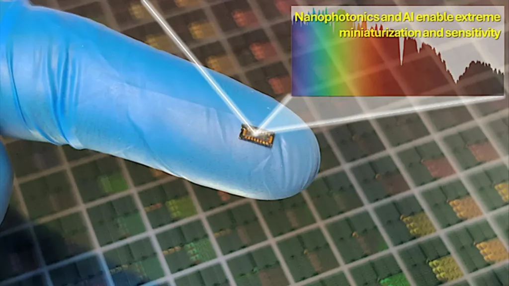
Now, a groundbreaking development from researchers at the University of California Davis (UC Davis) promises to fundamentally alter this landscape. Writing in the prestigious journal Advanced Photonics, the interdisciplinary team has unveiled a dramatically smaller, more efficient alternative: a spectrometer-on-a-chip so tiny it approaches the size of a single grain of sand. This innovation bypasses the conventional reliance on large optical components to physically separate light. Instead, the new system harnesses the power of artificial intelligence (AI) in conjunction with a minute array of specially engineered sensors to computationally reconstruct the full light spectrum. This paradigm shift from physical light dispersion to intelligent computational reconstruction represents a significant leap forward in photonics and analytical instrumentation.
The Historical Arc of Spectroscopy and the Drive for Miniaturization
Spectroscopy, the study of the interaction between matter and electromagnetic radiation, dates back to Isaac Newton’s experiments with prisms in the 17th century, where he demonstrated the dispersion of white light into its constituent colors. Over centuries, the field evolved dramatically, with pioneers like Joseph von Fraunhofer identifying dark lines in the solar spectrum in the early 19th century, laying the groundwork for modern analytical spectroscopy. By the 20th century, various spectroscopic techniques—from UV-Vis to Infrared (IR) and Raman spectroscopy—became indispensable tools across virtually every scientific discipline and industry.
However, despite their immense utility, traditional laboratory spectrometers have remained large, often tabletop-sized devices, requiring controlled environments and skilled operators. A high-end Fourier Transform Infrared (FTIR) spectrometer, for example, can occupy significant bench space, weigh dozens of kilograms, and cost tens of thousands of dollars. While smaller, portable versions have emerged in recent decades, they often sacrifice spectral resolution, range, or sensitivity, failing to meet the rigorous demands of many applications.
The relentless march of miniaturization, epitomized by the "lab-on-a-chip" movement, has long sought to shrink complex analytical systems onto microchips. The vision has been to enable point-of-care medical diagnostics, real-time environmental monitoring, and ubiquitous chemical analysis. Spectrometers, due to their optical path requirements, have historically been one of the most challenging instruments to miniaturize without compromising performance. This new UC Davis development directly addresses this long-standing challenge, pushing the boundaries of what is achievable in integrated photonics and AI-driven sensing.
Replacing Bulky Optics with AI-Driven Computation
The core ingenuity of the UC Davis chip lies in its radical departure from the standard method of physically spreading light into a rainbow. Instead of prisms or gratings, the system employs a mere 16 unique silicon detectors, each meticulously designed to react in a subtly different manner to incoming light. These detectors do not isolate individual colors directly; rather, they collect complex, encoded signals that collectively contain the hidden spectral information of the light source.
To conceptualize this process, one might consider the system as an assembly of highly specialized "tasters" sampling various nuanced aspects of the same complex mixture. Individually, each detector provides only a partial, seemingly incomplete piece of the overall picture. However, when their collective outputs are synergistically combined, they generate a rich dataset of information that is sufficient for the embedded artificial intelligence to reconstruct the original, full light spectrum with remarkable fidelity.
The second, equally critical component of this innovative architecture is a fully connected neural network. This AI model has been rigorously trained on thousands of examples, meticulously correlating the complex, often noisy, and highly encoded signals generated by the 16 detectors with their corresponding actual light spectra. This sophisticated training enables the AI to learn the intricate, non-linear relationship between these seemingly disparate signals and the true spectral composition of the light. This approach effectively solves what researchers in the field refer to as an "inverse problem"—a scenario where the desired output (the light spectrum) must be inferred from indirect measurements (the detector signals). By leveraging this AI-driven computational strategy, the system can reproduce spectral data with an impressive accuracy of approximately 8 nanometer (nm) resolution, all without the need for any bulky, traditional optical hardware. This computational approach not only facilitates miniaturization but also offers a pathway to potentially overcome inherent limitations of physical dispersion methods, such as signal-to-noise ratios and alignment sensitivities.
Expanding Silicon’s Reach into the Infrared Range
A major technical breakthrough underpinning this innovation involved the strategic modification of the surface of standard silicon photodiodes. Silicon, a cornerstone material in modern electronics and photonics, performs exceptionally well for detecting visible light (typically from 400 nm to 700 nm). However, its inherent material properties, specifically its bandgap, significantly limit its ability to efficiently capture near-infrared (NIR) light, typically wavelengths up to 1100 nm, where silicon becomes largely transparent.
The inability of standard silicon to detect NIR light has long been a bottleneck, as NIR light is particularly vital for a vast array of advanced applications. In biomedical imaging, for instance, NIR light is highly advantageous because it can penetrate much deeper into human tissue than visible light, enabling non-invasive diagnostics without significant scattering or absorption. This property is crucial for applications such as glucose monitoring, pulse oximetry, tissue oxygenation mapping, and even early cancer detection, where deeper tissue penetration is paramount. Beyond medicine, NIR spectroscopy is invaluable in agriculture for assessing crop health and soil composition, in food quality control for moisture and fat content, and in industrial process monitoring for chemical composition analysis.
The UC Davis team ingeniously circumvented this limitation by modifying the silicon photodiodes with specialized photon-trapping surface textures (PTSTs). These engineered PTST surfaces fundamentally alter how light behaves once it enters the chip. Instead of allowing NIR photons to simply pass straight through the thin silicon layer, the textured surface repeatedly scatters the light within the silicon. This internal scattering dramatically increases the optical path length of the NIR photons within the silicon material, significantly enhancing the likelihood that the silicon will absorb them. As a direct result of this innovative photon-trapping mechanism, the chip achieves sensitivity across a much wider spectral range than standard silicon sensors, extending its utility into the crucial near-infrared domain. This enhancement alone opens up a myriad of applications previously inaccessible to silicon-based miniaturized spectrometers.
Capturing Ultrafast Light Interactions: A New Frontier
Beyond its compact size and expanded spectral range, the new architecture offers another profound capability: the detection of ultrafast light interactions. The chip incorporates high-speed sensors specifically designed to measure photon lifetime with extremely high temporal precision. This advanced feature allows the device to detect transient, ultrafast interactions between light and matter that traditional spectrometers, limited by their inherent measurement speeds, might miss entirely.
Ultrafast spectroscopy operates on picosecond (10^-12 seconds) or even femtosecond (10^-15 seconds) timescales, enabling scientists to observe the dynamics of molecular vibrations, electron transfer, and chemical reactions as they happen. For example, understanding how energy flows through photovoltaic materials or how proteins fold involves processes occurring at these incredibly rapid speeds. The ability of this miniaturized spectrometer to capture such fleeting phenomena could revolutionize fields like materials science, photochemistry, and biophysics. Researchers associated with the project emphasize that this capability could unlock advanced forms of sensing and imaging that previously necessitated far larger, immensely complex, and prohibitively expensive femtosecond laser systems and specialized detectors, typically confined to advanced research laboratories. This integration of ultrafast detection into a chip-scale device marks a significant democratization of advanced spectroscopic capabilities.
Tiny Footprint with Big Potential: Implications and Market Impact
The completed UC Davis system is a marvel of engineering, occupying a minuscule footprint of just 0.4 square millimeters. Despite its diminutive size, it maintains high sensitivity and exhibits strong resistance to electrical noise, a persistent and significant challenge for portable, low-cost electronic devices. Even in electromagnetically noisy environments, the AI-assisted design intelligently processes signals, preserving clear signal quality and ensuring robust performance.
The global market for spectroscopy equipment was valued at approximately USD 15.5 billion in 2022 and is projected to reach over USD 25 billion by 2030, driven by increasing demand in pharmaceutical, biotechnology, environmental, and food & beverage industries. A major growth driver in this market is the increasing adoption of portable and handheld analytical devices, which this UC Davis innovation is perfectly positioned to serve. The ability to perform complex spectral analysis outside the traditional laboratory setting is highly sought after, as it reduces costs, accelerates decision-making, and expands accessibility.
By seamlessly combining sophisticated machine learning algorithms with enhanced silicon light detection capabilities, this technology is poised to pave the way for a new generation of compact, real-time hyperspectral sensing devices. Hyperspectral imaging, which collects and processes information across the electromagnetic spectrum, has typically required highly specialized and expensive cameras. Integrating such capabilities into a grain-of-sand-sized chip opens up unprecedented possibilities.
The potential applications are vast and transformative, spanning numerous sectors:
- Portable Medical Diagnostics and Wearable Health Monitors: Imagine a wearable device capable of non-invasively monitoring blood glucose levels with high accuracy, or detecting early markers of disease through subtle changes in tissue composition. This technology could enable continuous, real-time health monitoring, moving diagnostics from clinics to patients’ daily lives. It could also facilitate point-of-care testing in remote areas, democratizing access to advanced medical analysis.
- Environmental Remote Sensing: Miniaturized spectrometers could be deployed in drones, autonomous vehicles, or fixed sensors for real-time monitoring of air and water quality, detecting pollutants, greenhouse gases, and chemical spills with unprecedented spatial and temporal resolution. This would allow for proactive environmental management and rapid response to ecological threats.
- Food Quality Analysis and Safety: From verifying the authenticity of olive oil to detecting pesticide residues on produce, or assessing the ripeness and nutritional content of fruits, this chip could provide instant, on-site analysis, enhancing food safety and supply chain efficiency. It could also help combat food fraud, a multi-billion-dollar global issue.
- Industrial Process Control: Integrating these tiny spectrometers directly into manufacturing lines could enable real-time quality control, monitoring chemical reactions, material composition, and product consistency, leading to greater efficiency, reduced waste, and improved product reliability.
- Security and Defense: Rapid detection of explosives, illicit drugs, or chemical agents at checkpoints or in the field could be significantly enhanced by such compact, robust analytical tools.
Speaking on the implications, a lead researcher from the UC Davis team, who wished to remain unnamed pending further patent filings and commercialization discussions, commented, "This isn’t just about making spectrometers smaller; it’s about making them ubiquitous. We’re moving from a paradigm where you bring the sample to the instrument, to one where the instrument can go to the sample, wherever it may be. The integration of AI is not just an add-on; it’s fundamental to how this device functions, allowing us to extract rich spectral information from minimal physical interaction with light."
The development represents a significant stride in the field of integrated photonics, demonstrating the profound synergistic potential when advanced materials engineering is combined with cutting-edge artificial intelligence. As research progresses towards mass production and further optimization, the UC Davis spectrometer-on-a-chip is poised to become a foundational technology, enabling a new era of pervasive, intelligent sensing that could redefine how we interact with and understand the world around us. Its impact is expected to resonate across scientific research, industrial innovation, and daily life, marking a pivotal moment in the quest for truly smart, connected analytical tools.