The pervasive issue of overheating, a phenomenon familiar to any laptop user, represents a critical barrier to the advancement of global computing infrastructure, from individual consumer devices to the massive server farms powering the internet. As semiconductor manufacturers strive to make computer chips more compact and powerful, the density of transistors increases, leading to higher localized temperatures that can degrade performance or cause catastrophic hardware failure. While the macro-scale effects of heat are well-documented, the micro-scale movement of thermal energy through the complex, multilayered architectures of modern electronics has remained notoriously difficult to observe. In a breakthrough study recently published in Nature Communications, researchers at the Massachusetts Institute of Technology (MIT) have demonstrated a novel diagnostic method that utilizes high-intensity X-rays and ultrafast laser pulses to visualize heat dissipation at the nanoscale. By providing a clear view of how heat navigates through internal layers and encounters microscopic defects, this technique offers a roadmap for designing more resilient and power-dense electronics for artificial intelligence, wearable technology, and clean energy systems.
The Thermal Bottleneck in Modern Semiconductor Design
For decades, the semiconductor industry followed the trajectory of Moore’s Law, doubling the number of transistors on a microchip approximately every two years. However, as the industry approaches the physical limits of silicon, a new challenge has emerged: the "thermal wall." When transistors are packed into increasingly smaller areas, the heat generated during their operation becomes more concentrated. Without efficient dissipation, this heat creates "hotspots" that can throttle processing speeds or damage the delicate atomic structure of the chip.
In large-scale data centers, which are the backbone of the modern digital economy, heat management is an existential challenge. Current estimates suggest that cooling systems account for nearly 40 percent of the total energy consumption in these facilities. As AI applications demand more intensive computational power, the energy required to keep servers within safe operating temperatures is projected to rise exponentially. Understanding the fundamental physics of heat transport is therefore not just a matter of improving laptop battery life, but a necessity for global energy sustainability.
The primary obstacle for engineers has been the inability to see what is happening inside a chip. Modern electronics are not monolithic blocks; they are sophisticated "sandwiches" composed of five or more layers of different materials, including semiconductors, insulators, and metallic interconnects. Traditional thermal measurement techniques often fail when applied to these multilayered structures, as they cannot penetrate beneath the surface or distinguish between the thermal signatures of different layers.
Limitations of Existing Thermal Diagnostic Tools
Before the MIT breakthrough, researchers relied on several established methods to model and measure heat flow, each with significant drawbacks. One of the most common optical methods is Time Domain Thermal Reflectance (TDTR). This technique uses a laser to heat the surface of a material and then measures the change in reflectivity to infer temperature. However, TDTR is primarily a surface-level diagnostic. Because it relies on visible light, it cannot effectively "see" through the opaque layers of a real-world electronic device. It provides an average signal for the entire stack, making it impossible for engineers to pinpoint which specific layer or interface is obstructing heat flow.
Other methods, such as infrared thermography, are hampered by their resolution and speed. While infrared cameras can provide a broad map of a device’s temperature, they lack the spatial resolution to see features at the micrometer or nanometer scale. Furthermore, they cannot capture the ultrafast thermal transients—the split-second spikes in temperature—that occur during high-speed computing cycles.
"When doing these diagnoses using traditional techniques, they couldn’t get down to the micro- or nanometer scale," explains Mingda Li, an associate professor of nuclear science and engineering at MIT and co-corresponding author of the study. "But eventually, they’d like to go beyond that to study the heat carriers and understand exactly what causes failure, in order to avoid local hotspots and design better devices. This approach is a step in that direction."
The MIT Solution: Combining X-Rays and Laser Pulses
To overcome these visibility barriers, the MIT research team, in collaboration with scientists from Argonne National Laboratory and the University of Texas at Austin, turned to the unique properties of X-rays. Unlike visible light, high-energy X-rays can penetrate deep into multilayered materials, providing information about the internal atomic structure through a process called X-ray diffraction.
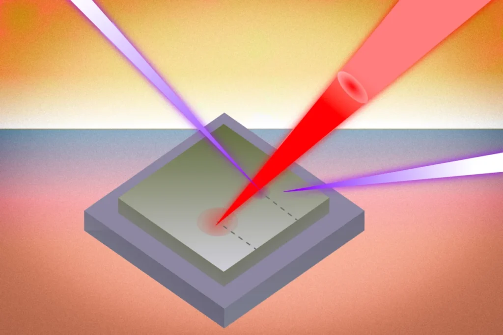
The researchers utilized one of the brightest X-ray sources in the world, located at a national laboratory facility, to focus a beam with incredibly fine spatial resolution. The experimental setup involved a "pump-probe" technique: a laser pulse (the "pump") was used to deliver a precise burst of heat to the sample, while the ultrafast X-ray pulses (the "probe") scanned the material in real-time.
As the laser heats the material, the atoms within the crystal lattice begin to vibrate and expand, creating "strain." By measuring how the X-rays diffract off these vibrating atoms, the researchers could calculate the exact temperature and heat flow within specific layers of the device. This allowed them to distinguish between the thermal behavior of the top layer and the layers buried deep beneath the surface.
"X-rays can clearly show how heat propagates across the interface through their diffraction," says Chuliang Fu, an MIT postdoc and co-lead author. This capability is vital because the interfaces—the points where two different materials meet—are often where the most significant thermal resistance occurs.
Case Study: Gallium Nitride and the Impact of Micro-Defects
The research team applied their new technique to a test device composed of Gallium Nitride (GaN) grown on a silicon substrate. GaN is a "wide-bandgap" semiconductor that is increasingly replacing traditional silicon in power electronics and 5G infrastructure because it can handle higher voltages and conduct heat more efficiently. However, the manufacturing process for GaN often introduces tiny defects, such as "wrinkles" or dislocations, which occur when the GaN crystal lattice does not perfectly align with the silicon base.
Using their X-ray technique, the MIT team was able to quantify the thermal impact of a single micron-scale wrinkle defect. The results were startling: they measured a fourfold (400 percent) reduction in the material’s ability to transfer heat at the site of the defect. Furthermore, they discovered that the defect caused heat to spread unevenly, or anisotropically. Instead of dissipating in a circular pattern, the heat moved much more easily in one direction than the other, effectively creating a thermal "bottleneck" that could lead to a localized hotspot.
"When people model heat dissipation, they model perfect crystals without defects," says Mingda Li. "But these types of large wrinkle defects are very common in 2D materials. People never even knew how much heat is blocked by these wrinkles. Those are things we can now directly observe with this technique."
The study also revealed a 25 percent overall drop in heat dissipation across the material interfaces compared to theoretical models. This suggests that even "minor" processing imperfections have a far greater impact on device reliability than previously assumed by the industry.
Chronology of Thermal Management Research
The development of this X-ray technique marks a significant milestone in the history of thermal management research. To understand its importance, one must look at the evolution of the field:
- 1960s-1980s: Thermal management focused on macro-scale solutions, such as larger aluminum heat sinks and more powerful fans.
- 1990s: The introduction of heat pipes and liquid cooling for high-end workstations and servers.
- 2000s: The development of Time Domain Thermal Reflectance (TDTR) allowed researchers to begin measuring thermal properties at the microscopic level, though limited to surfaces.
- 2010s: The rise of "2D materials" like graphene and Gallium Nitride highlighted the need for better interface management.
- 2020-Present: The integration of AI and 3D chip stacking (heterogeneous integration) created a crisis in thermal density.
- 2024: MIT’s demonstration of sub-surface X-ray thermal mapping provides the first "high-definition" view of internal heat transport.
Industry Implications and Official Responses
The semiconductor industry has already shown intense interest in the MIT findings. A leading semiconductor industry consortium has reportedly reached out to the research team to explore how this measurement technique can be applied to commercial chip designs.
Jeehwan Kim, an MIT associate professor and co-corresponding author, emphasizes that the industry has been waiting for a tool that can provide direct experimental measurements of real-world devices. "We can now pass a current and shine an X-ray on a device and see how the heat dissipates at a very small scale. That’s something the industry has been longing for."
The implications extend beyond just cooling. By understanding exactly where heat is trapped, companies can:
- Optimize Geometry: Design the layout of transistors and interconnects to avoid "shadowing" effects where one component blocks the cooling path of another.
- Improve Material Selection: Identify which specific manufacturing processes or material combinations produce the fewest thermal-blocking defects.
- Enhance AI Hardware: Develop more power-dense AI accelerators that can run at higher clock speeds without the risk of thermal failure.
- Advance Wearables: Ensure that high-performance chips in smartwatches or medical sensors do not reach temperatures that could cause discomfort or skin burns for the user.
Analysis: The Future of Thermal-Aware Design
The work conducted by the MIT team represents a shift from "reactive" to "proactive" thermal design. In the past, engineers would build a chip and then figure out how to cool it. With this new diagnostic tool, the era of "thermal-aware design" begins. Engineers can now model the thermal consequences of every manufacturing decision with atomic-level precision.
Furthermore, this technique will be instrumental in the development of "clean energy" systems. High-power inverters used in electric vehicles and solar power grids rely on materials like GaN and Silicon Carbide. If these components can be made more thermally efficient, they will become more reliable and lose less energy as waste heat, directly contributing to the efficiency of the green energy transition.
The research was a multi-institutional effort, supported by the U.S. Department of Energy and the National Science Foundation, underscoring its importance to national technological infrastructure. As the team continues to refine the method, they hope to transition it from specialized national laboratories to more accessible industrial settings, potentially revolutionizing how every future microchip is tested and validated.
In the words of Professor Jeehwan Kim, "This will enable better thermal design of electronic systems. Even with the same type of materials, the geometry and how the materials are laid out is quite complicated, so it will show us how those differences impact thermal flow by providing direct experimental measurements." By lifting the veil on the internal "weather patterns" of heat inside a chip, MIT has provided the industry with the clarity needed to continue the march toward smaller, faster, and cooler technology.