For decades, the relentless pursuit of smaller and more powerful electronic components has served as the primary engine for monumental advancements in technology, driving everything from supercomputers to the smartphones in our pockets. This foundational principle, famously encapsulated by Moore’s Law, has seen the number of transistors on integrated circuits double approximately every two years. As silicon-based technologies approach their fundamental physical limits, scientists globally have intensified their search for the next paradigm shift in computer chip design. Amidst this quest, two-dimensional (2D) materials, characterized by their ultrathin structures comprising just one or a few atomic layers, have emerged as highly promising candidates for constructing the next generation of even tinier, more efficient electronic devices. Their unique electronic and mechanical properties, such as high electron mobility in graphene or tunable band gaps in transition metal dichalcogenides like molybdenum disulfide (MoS2), have fueled widespread optimism within the scientific and industrial communities.
However, groundbreaking new research emanating from TU Wien in Austria suggests a critical, previously underestimated challenge that could significantly impede the real-world application of many of these highly anticipated 2D materials in chip technology. The problem, as identified by the TU Wien team, does not lie solely within the intrinsic properties of the 2D materials themselves. Instead, their findings reveal a fundamental issue arising from the necessary integration of 2D materials with insulating layers—typically oxides—which are indispensable for the functioning of any electronic device. An unavoidable atomic-scale gap, a minuscule separation, forms between the 2D material and its insulating counterpart. This tiny, yet critically significant, separation has been shown to drastically reduce device performance and, more importantly, poses a fundamental physical barrier to further miniaturization, potentially redirecting billions of dollars in research and development investment within the semiconductor industry.
The Relentless March of Miniaturization: A Historical Perspective
The history of computing is inextricably linked with the narrative of miniaturization. From the bulky vacuum tube computers of the mid-20th century to the integrated circuits of today, each successive generation has seen components shrink, leading to exponential increases in processing power and reductions in energy consumption. Gordon Moore’s observation in 1965, later termed Moore’s Law, became the guiding principle for the semiconductor industry, predicting a doubling of transistor density every 18-24 months. This prediction held remarkably true for over five decades, driven by innovations in photolithography, materials science, and device architecture.
The global semiconductor industry, valued at approximately $573.5 billion in 2022 and projected to exceed $1 trillion by 2030, thrives on this continuous innovation. Companies like Intel, TSMC, Samsung, and NVIDIA invest tens of billions annually in research and development to push the boundaries of chip manufacturing. For instance, Intel alone reported R&D expenditures of over $17 billion in 2022, a significant portion of which is dedicated to exploring next-generation materials and fabrication techniques. As silicon-based transistors reach atomic-scale dimensions, physical phenomena such as quantum tunneling and increased heat generation pose severe limitations. This impending "end of Moore’s Law" for conventional silicon has spurred an urgent global race to discover and implement alternative materials and architectures. It is within this context that 2D materials rose to prominence, offering a potential escape route from the scaling challenges of silicon.
The discovery of graphene in 2004 by Andre Geim and Konstantin Novoselov at the University of Manchester, which earned them the Nobel Prize in Physics in 2010, ignited immense excitement. Graphene, a single atomic layer of carbon atoms arranged in a hexagonal lattice, exhibited extraordinary electrical conductivity, mechanical strength, and thermal properties. This breakthrough opened the floodgates for research into a plethora of other 2D materials, including transition metal dichalcogenides (TMDs) like molybdenum disulfide (MoS2), tungsten diselenide (WSe2), and hexagonal boron nitride (h-BN). These materials offered diverse electronic properties, from metallic to semiconducting to insulating, making them theoretically ideal building blocks for a wide range of future electronic devices, from ultra-low power transistors to flexible electronics and advanced sensors.
A Fundamental Barrier Emerges: The Atomic-Scale Gap
The optimism surrounding 2D materials has been palpable, with countless studies focusing on their intrinsic properties. However, the new research from TU Wien, conducted by Professor Mahdi Pourfath and Professor Tibor Grasser at the Institute for Microelectronics, shifts the focus from the isolated material to its behavior within a complete device structure. "For many years, researchers have quite rightly been fascinated by the remarkable electronic properties of novel 2D materials such as graphene or molybdenum disulfide," explains Prof. Pourfath. "What is often overlooked, however, is that a 2D material alone does not make an electronic device. We also need an insulating layer — usually an oxide. And this is where things become more complicated from a materials science perspective."
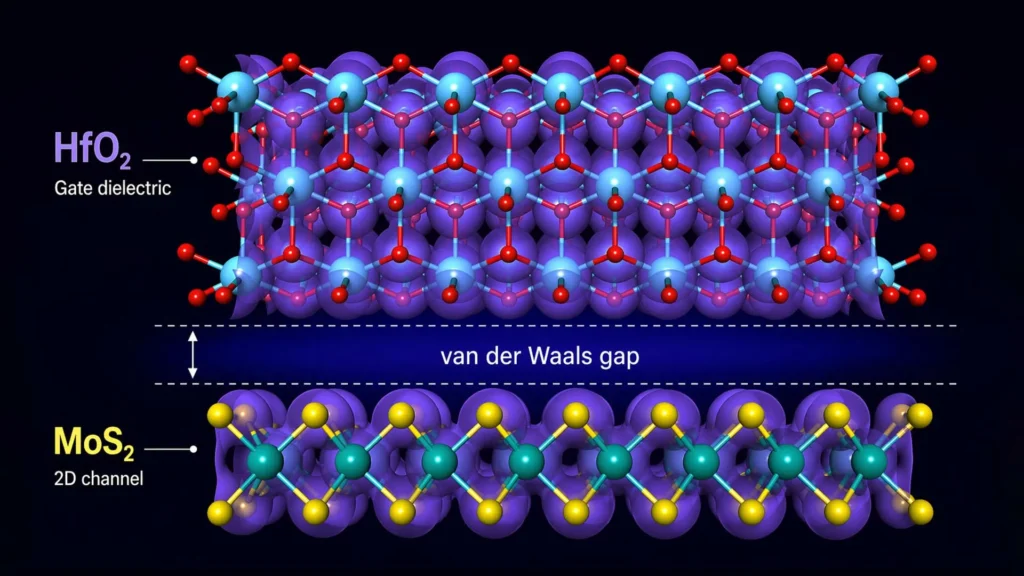
Modern transistors operate by switching a semiconductor material between conductive (ON) and nonconductive (OFF) states. In future chips aiming for unprecedented miniaturization, this semiconductor role could be filled by an ultrathin 2D material. The crucial switching action is controlled by a gate electrode, which must be electrically isolated from the active semiconductor channel by an insulating layer, known as a gate dielectric. To achieve maximum device density and efficiency, this insulating layer also needs to be exceptionally thin. It is precisely this requirement for ultrathin insulation that exposes the critical issue.
The TU Wien team’s simulations and analysis revealed that in numerous combinations of 2D materials and common insulating layers, the bonding mechanism between them is fundamentally weak. "In many combinations of 2D materials and insulating layers, the bonding between them is relatively weak," elaborates Prof. Grasser. "They are held together only by so-called van der Waals forces, which provide only a weak attraction between the semiconductor and the insulator. As a result, the two layers do not come into close contact — there is always a gap between them."
This "van der Waals gap," though minuscule, measures approximately 0.14 nanometers. To put this into perspective, a single sulfur atom has a diameter of about 0.2 nanometers, and a SARS-CoV-2 virus is roughly 700 times larger than this gap. Despite its incredibly small size, this atomic-scale separation has a profound and detrimental effect on the electronic behavior of the integrated device. The gap significantly weakens the capacitive coupling between the 2D material and the gate dielectric. In a transistor, effective capacitive coupling is essential for the gate electrode to efficiently control the flow of current through the semiconductor channel. A weaker coupling means that the gate loses its ability to effectively switch the device, leading to degraded performance, higher power consumption, and ultimately, a failure to meet the stringent requirements for next-generation computing.
The Crucial Role of Interfaces: Why Device Integration Matters
The findings underscore a critical oversight in much of the preceding research on 2D materials. Many studies have predominantly concentrated on characterizing the impressive intrinsic properties of these materials in isolation, often under ideal laboratory conditions. Less attention has been paid to the complex, atomic-scale interactions that occur at the interfaces when these materials are integrated into a functional device structure. The TU Wien research unequivocally demonstrates that these interfaces, rather than just the standalone material properties, may ultimately determine the success or failure of future chip technologies employing 2D materials.
Industry experts and materials scientists have long acknowledged the challenges of integrating novel materials into existing semiconductor manufacturing processes. However, the revelation of a fundamental physical gap, unavoidable with weak van der Waals bonding, adds a new layer of complexity. This isn’t merely a manufacturing defect to be engineered away; it’s an inherent property of certain material combinations. This realization could prevent the semiconductor industry from expending substantial financial resources—potentially billions of dollars—on research avenues that, due to these physical limitations, may never yield viable commercial solutions for extreme miniaturization.
Industry Implications and Strategic Recalibration
The implications of this research for the global semiconductor industry are substantial. With the immense investment in 2D materials research over the past decade, a clear understanding of fundamental limitations is paramount. Chip manufacturers and research consortia, suchating IMEC (Interuniversity Microelectronics Centre) and SRC (Semiconductor Research Corporation), routinely fund exploratory research into novel materials. The TU Wien findings serve as a crucial guiding post, indicating which material combinations are likely to face insurmountable physical hurdles.
For instance, major players like Intel, TSMC, and Samsung are constantly evaluating new materials for their roadmap beyond current silicon nodes (e.g., 3nm, 2nm, and below). Their materials science divisions, often collaborating with academic institutions, would need to integrate these findings into their strategic planning. This might lead to a redirection of research efforts away from 2D material/insulator pairs that rely solely on weak van der Waals interactions towards alternatives that promise stronger atomic bonding.
"Our work is good news for the semiconductor industry," says Tibor Grasser. "We can predict which materials are suitable for future miniaturization steps — and which are not. But if one focuses only on the 2D materials themselves, without considering the unavoidable insulating layers from the outset, there is a risk of investing billions in an approach that simply cannot succeed for fundamental physical reasons." This statement highlights the financial prudence this research offers, potentially saving the industry from costly dead ends.
"Zipper Materials": A Path Forward for 2D Electronics
While the research identifies a significant challenge, it also points towards a potential solution: the deliberate design of interfaces. The key lies in moving beyond materials that interact only via weak van der Waals forces. Instead, the focus should shift to systems where the semiconductor and insulating layers bond together much more strongly, effectively eliminating the problematic gap. The TU Wien team refers to these as "zipper materials" – a concept where the layers are tightly interlocked at the atomic level, similar to how a zipper functions.
"If the semiconductor industry wants to succeed with 2D materials, the active layer and the insulating layer must be designed together from the very beginning," emphasizes Mahdi Pourfath. This calls for a holistic approach to materials selection and device architecture, where the interface properties are considered as critically as the intrinsic properties of the individual layers. Developing such "zipper materials" would involve exploring new material chemistries and fabrication techniques that promote strong covalent or ionic bonding across the interface. This could involve, for example, functionalizing the surfaces of 2D materials or using specific growth methods that encourage direct chemical bonding with the dielectric.
Examples of such research directions might include exploring atomic layer deposition (ALD) techniques to grow dielectrics directly onto 2D materials, aiming for chemical bonds rather than physical adsorption. Another avenue could be the development of novel 2D heterostructures where different 2D materials are chosen not just for their electronic properties but also for their ability to form strong, gap-free interfaces with specific dielectric layers.
Redefining the Search for Next-Generation Chips
The TU Wien research marks a pivotal moment in the ongoing quest for next-generation computer chips. It reframes the discussion around 2D materials, moving it from a focus on individual material prowess to the intricate dynamics of integrated device structures. It serves as a powerful reminder that in the nanoscale world, even the smallest atomic-scale imperfections can have profound macroscopic consequences.
This work will undoubtedly influence the strategic roadmaps of major semiconductor research institutions and corporations. It calls for a more integrated and interface-aware approach to materials science and device engineering. Rather than simply screening 2D materials for their theoretical performance, researchers will now need to prioritize their compatibility with insulating layers and their ability to form stable, strong interfaces.
The future of computing continues its trajectory towards greater density, speed, and energy efficiency. While the promise of 2D materials remains immense, the TU Wien findings provide a critical reality check and a clear direction forward. By understanding and actively engineering the atomic-scale interfaces, the semiconductor industry can avoid costly missteps and effectively harness the revolutionary potential of 2D materials, ensuring that the relentless march of miniaturization continues, albeit with a more nuanced and integrated scientific approach. The "zipper materials" concept offers a tangible pathway, demanding innovative chemistry and precise engineering to unlock the full capabilities of these ultrathin marvels and drive the next wave of technological breakthroughs.