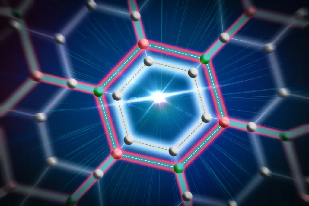
A multidisciplinary team of researchers at the Massachusetts Institute of Technology (MIT) and several partner institutions has achieved a significant breakthrough in the field of quantum materials by developing a scalable method to produce air-stable, monolayer-thick superconductors. The research, published today in the journal Nature, describes a novel "grown-at-interface" fabrication process that allows for the creation of ultra-thin niobium diselenide ($NbSe_2$) films that retain their superconducting properties even when exposed to ambient air. This advancement addresses a decade-long hurdle in the development of next-generation quantum hardware, potentially paving the way for the miniaturization of quantum circuits and the creation of hypersensitive detectors for use in telecommunications and cosmological research.
The Quest for Two-Dimensional Superconductors
Superconductors are a class of materials capable of conducting electricity with zero resistance when cooled below a specific critical temperature. This property is fundamental to the operation of modern quantum computers, which rely on superconducting circuits to maintain the delicate quantum states of qubits. Traditionally, these circuits have been constructed using "bulk" materials—substances that are many thousands of atoms thick. However, as the demand for more powerful and compact quantum processors grows, scientists have turned their attention to two-dimensional (2D) materials.
Two-dimensional superconductors, which consist of a single layer of atoms, offer unique physical properties that their bulk counterparts lack. Among these, niobium diselenide ($NbSe_2$) has emerged as a material of particular interest. A single layer of $NbSe_2$ consists of niobium atoms sandwiched between two layers of selenium atoms. Despite being only about one nanometer thick, this material exhibits an extraordinarily high "kinetic inductance." Kinetic inductance is a phenomenon where the inertia of charge carriers (Cooper pairs in a superconductor) allows the material to store magnetic energy. In quantum electronics, high kinetic inductance is a vital resource, as it allows for the creation of compact inductive elements that are essential for qubit design and signal processing.
Despite its potential, $NbSe_2$ has historically been plagued by extreme instability. When removed from the inert, vacuum-controlled environments in which it is synthesized, the material oxidizes almost instantly upon contact with oxygen or moisture in the air. This degradation destroys its superconducting properties, rendering it useless for practical applications. Until now, researchers were forced to rely on "exfoliation"—the manual peeling of small flakes from a larger crystal—which produced inconsistent results and materials too small for industrial-scale manufacturing.
A Paradigm Shift: The Grown-Under-Graphene Method
The MIT-led team, which included researchers from New York University, Rice University, Yale University, and Pohang University of Science and Technology, recognized that the traditional "growth then protect" workflow was fundamentally flawed. Typically, scientists would grow the superconductor and then attempt to lay a protective layer, such as graphene or hexagonal boron nitride, on top. However, the nanoseconds of exposure during the transfer process were often enough to initiate degradation.
To circumvent this, the researchers inverted the process. They first placed a layer of graphene onto a silicon dioxide ($SiO_2$) substrate. Although graphene adheres to the substrate, the atomic-level "weak adhesion" between the two materials leaves a microscopic gap—less than one nanometer in height. The researchers then introduced chemical precursors into this environment. Under precisely controlled conditions, the $NbSe_2$ crystal began to grow within this tiny gap, effectively using the graphene as a pre-installed protective "roof."
"It took a long time for us to understand how the growth could happen underneath the graphene," said co-lead author Xudong Sheldon Zheng, a graduate student in the MIT Department of Electrical Engineering and Computer Science (EECS). "Through collaboration and discussion, we eventually uncovered the mechanism for growing the material at the interface, and this solves a lot of problems and allows us to simplify our fabrication steps."
The silicon dioxide substrate serves a dual purpose: it traps the chemical precursors long enough for the crystal to nucleate, while the graphene layer provides a smooth surface that allows the atoms to migrate and form a continuous, uniform monolayer. This method allowed the team to produce smooth films of $NbSe_2$ exceeding one inch in size—a "wafer-scale" achievement that represents a massive leap over the micron-sized flakes produced by exfoliation.
Overcoming the Integration Hurdle
Producing a stable material is only the first half of the challenge; the second is integrating that material into a functional electronic circuit. Because the $NbSe_2$ layer is only one nanometer thick, creating a reliable electrical connection with standard metal electrodes (which are often hundreds of nanometers thick) is a delicate task.
The researchers developed an "oxidation-free transfer technique" to move the graphene-superconductor sandwich from the growth substrate to a circuit board. To ensure a clean contact, they employed a vacuum-based etching process. By carefully etching the side walls of the thin film, they created a "one-dimensional contact" along the edge of the material. This method preserves the integrity of the superconducting layer while ensuring that electrons can flow freely between the monolayer and the macroscopic circuit components.
When the integrated circuit was tested, the results were definitive. The $NbSe_2$ maintained its superconducting state and demonstrated the high kinetic inductance that the researchers had theorized. This confirmed that the "grown-at-interface" process did not compromise the material’s internal physics, making it a viable candidate for high-performance quantum devices.
Supporting Data and Technical Analysis
The implications of high kinetic inductance cannot be overstated in the context of quantum circuit design. Currently, many quantum devices achieve high inductance by using arrays of Josephson junctions—complex structures consisting of two superconductors separated by a thin insulator. While effective, these arrays take up significant "real estate" on a quantum chip.
By utilizing monolayer $NbSe_2$, engineers can replace these bulky arrays with a single, tiny strip of 2D material. This could lead to a reduction in circuit footprint by several orders of magnitude. For example, a standard superconducting resonator used in quantum computing might be reduced from millimeters in length to just a few micrometers.
The study’s data also highlighted the uniformity of the grown films. Unlike exfoliated flakes, which vary in thickness and quality, the CVD-grown (Chemical Vapor Deposition) films under graphene showed remarkable consistency across the entire wafer. This uniformity is a prerequisite for any technology intended for mass production, as it ensures that every device on a chip performs identically.
Chronology of 2D Superconductor Development
The journey to this discovery follows a decade of incremental progress in the field of "Van der Waals" materials:
- 2004: The isolation of graphene sparks global interest in 2D materials.
- 2010-2015: Researchers identify that Transition Metal Dichalcogenides (TMDs), like $NbSe_2$, can exhibit superconductivity in their bulk form and as thin flakes.
- 2016-2020: Studies confirm that $NbSe_2$ remains superconducting even at the monolayer limit, but researchers struggle with its rapid oxidation in air.
- 2021-2023: Various "encapsulation" methods are attempted, but none successfully scale the material to wafer sizes without degradation.
- 2024: The MIT team perfects the "interface growth" method, publishing their results in Nature and demonstrating the first air-stable, wafer-scale integration.
Broader Impact and Future Implications
The ability to manufacture stable, ultra-thin superconductors at scale has wide-ranging implications beyond the laboratory.
1. Quantum Computing Scalability:
The primary bottleneck for quantum computers is the physical size of the hardware. To solve real-world problems, quantum computers will eventually need millions of qubits. Using current bulk-superconductor technology, such a machine would be prohibitively large. The miniaturization enabled by $NbSe_2$ is a critical step toward fitting more quantum power into a smaller space.
2. Advanced Communications:
Superconducting nanowire single-photon detectors (SNSPDs) are the gold standard for secure quantum communications. High kinetic inductance materials can improve the sensitivity and timing resolution of these detectors, facilitating faster and more secure data transmission across global networks.
3. Cosmology and Fundamental Physics:
Scientists searching for dark matter or studying the Cosmic Microwave Background (CMB) require detectors capable of sensing infinitesimal amounts of energy. The high inductance and low noise of monolayer superconductors make them ideal for these "ultrasensitive" applications.
4. Material Science Expansion:
Importantly, the researchers noted that their growth strategy is not limited to $NbSe_2$. The "grown-under-graphene" technique can likely be applied to a broad family of other 2D materials that are currently too unstable for practical use. This opens up a new "library" of materials for scientists to explore.
Official Responses and Collaborative Efforts
The study was a massive collaborative effort, reflecting the interdisciplinary nature of modern physics. Corresponding authors included William D. Oliver, a professor of physics and EECS at MIT and a leading figure in quantum engineering; Joel I-Jan Wang, an assistant professor at New York University; and Jing Kong, an MIT professor known for her work in chemical vapor deposition.
"Emerging superconductors that are only a monolayer thick have a lot of potential," said Xudong Sheldon Zheng. "Thanks to our new process, they are no longer materials that can only be made at a very small scale. There are now exciting opportunities for scientists to study these materials, utilize them in circuits, and explore their practical applications."
Sameia Zaman, an EECS graduate student and co-lead author, emphasized the future of the research. "We’ve taken a very good step toward exploring both the physics and the application side of this thin, monolayer superconductor… There are a lot of directions we can go in the future."
The research was supported by a diverse group of funders, including the U.S. Army Research Office, the National Science Foundation, the Department of Energy, and the National Research Foundation of Korea. This broad support underscores the strategic importance of quantum material science to both national security and global technological progress.
As the team moves forward, their next goal is to integrate these materials into more complex, functional device architectures. By moving from simple circuits to full-scale quantum processors, the researchers hope to turn the theoretical promise of 2D superconductors into a tangible reality that transforms the landscape of 21st-century technology.