For decades, ultrafast lasers have stood as formidable instruments at the vanguard of modern optics. Their characteristic pulses, fleeting for mere hundreds of femtoseconds—quadrillionths of a second—have underpinned a revolutionary suite of technologies. These range from the micron-level precision required in advanced manufacturing and the delicate accuracy demanded by modern eye surgery to the foundational principles of optical frequency combs, the Nobel Prize-winning innovation that is instrumental in powering the world’s most accurate optical atomic clocks. Yet, despite their profound impact and versatility, these indispensable tools have largely remained tethered to their origins as substantial, high-cost systems, typically occupying entire optical tables within specialized laboratories. This physical and financial barrier has, until now, limited their broader dissemination and integration into more compact, accessible platforms.
A significant paradigm shift is now on the horizon, thanks to groundbreaking research emanating from EPFL (École Polytechnique Fédérale de Lausanne). A team led by Professor Tobias J. Kippenberg has unveiled a breakthrough that promises to dramatically condense this powerful technology. In a landmark publication featured in the prestigious scientific journal Nature, the researchers report the successful development of the first integrated ultrafast laser capable of rivaling the performance benchmarks traditionally set by their tabletop counterparts. This innovative device achieves impressive pulse energies of 1.05 nanojoules and pulse durations as brief as 147 femtoseconds, all while being contained within a compact photonic chip. This achievement marks a pivotal moment, signaling a potential future where the extraordinary capabilities of ultrafast lasers are no longer confined to expansive laboratories but are instead miniaturized and made accessible for a myriad of new applications.
The Enduring Power of Ultrafast Lasers: A Legacy of Precision
To fully appreciate the magnitude of this breakthrough, it is essential to understand the unique characteristics and widespread applications of ultrafast lasers. A femtosecond (fs) is an almost unimaginably short duration of time, equal to 10^-15 seconds. To put this into perspective, there are more femtoseconds in a single second than there have been seconds in the entire history of the universe. In this minuscule timeframe, light travels only about 0.3 micrometers, a distance smaller than the diameter of a typical bacterium. This extreme temporal brevity grants ultrafast lasers unparalleled capabilities.
In precision manufacturing, these lasers are used for micro-machining, drilling, and cutting materials with minimal heat damage, enabling the creation of intricate components for electronics, medical devices, and aerospace. Their ability to ablate material without significant thermal diffusion allows for "cold ablation," which is crucial for processing heat-sensitive materials and achieving superior surface quality. For instance, they are vital in fabricating microfluidic devices, creating stents, and manufacturing components for smartphones.
In medicine, particularly ophthalmology, femtosecond lasers have revolutionized eye surgery. Procedures such as LASIK (Laser-Assisted In Situ Keratomileusis) rely on these lasers to create precise corneal flaps, while femtosecond laser-assisted cataract surgery offers enhanced accuracy and predictability compared to traditional methods. Beyond surgery, their diagnostic potential in non-invasive imaging, such as optical coherence tomography (OCT), is continually expanding.
Perhaps one of the most intellectually profound applications lies in optical frequency combs. Awarded the Nobel Prize in Physics in 2005 to John L. Hall and Theodor W. Hänsch, this innovation allows for the precise measurement of optical frequencies, effectively acting as an "optical ruler." Frequency combs are central to the operation of optical atomic clocks, which are orders of magnitude more accurate than their microwave predecessors. Current optical atomic clocks can achieve an accuracy of one part in 10^18, meaning they would lose or gain only one second in billions of years. Such unprecedented precision is vital for next-generation global navigation satellite systems (GPS), quantum computing, fundamental physics research (e.g., testing general relativity), and secure communication networks.
Despite these transformative applications, the intrinsic nature of ultrafast laser systems—involving complex optical cavities, bulky pump lasers, and elaborate cooling mechanisms—has meant that they typically occupy large optical tables, often several meters in length and width, and can cost anywhere from tens of thousands to well over a million dollars, plus significant maintenance overhead. This physical footprint and financial barrier have been the primary impediments to their widespread adoption outside of specialized research and industrial settings.
The Miniaturization Imperative: Integrated Photonics at the Forefront
The quest for miniaturization has been a consistent driving force in technological advancement, from transistors to entire computing systems. In optics, this drive manifests as integrated photonics. Photonic chips, sometimes referred to as "light chips," manipulate light using microscopic structures known as waveguides, which are meticulously etched onto a semiconductor wafer. Analogous to how electronic chips route and process electrical signals through metallic traces, photonic chips guide, split, modulate, and process light signals.
These chips have already made significant inroads, particularly in telecommunications, where they have enabled the miniaturization of optical transceivers and other components, dramatically increasing data transfer rates and reducing the size and power consumption of network infrastructure. The underlying principle is to replace bulky discrete optical components—lenses, mirrors, prisms, and fibers—with their on-chip equivalents, thereby achieving higher integration density, improved stability, and lower manufacturing costs.
Professor Kippenberg succinctly articulated the long-standing ambition within the field: "For more than twenty years, a high-pulse-energy femtosecond laser on chip was widely regarded as a holy grail of integrated photonics." The term "holy grail" underscores the immense technical challenges involved in packing the complex physics of ultrafast pulse generation, amplification, and shaping into a silicon-compatible platform while maintaining performance comparable to free-space or fiber-based systems. The EPFL team’s success demonstrates that this elusive goal is not only attainable but can be achieved through an unexpectedly elegant design that had largely been overlooked by the integrated photonics community.
An Overlooked Design Delivers: The Mamyshev Oscillator’s Renaissance
The key to this breakthrough lies in the researchers’ astute adoption of a laser architecture known as the Mamyshev oscillator. Developed in the 1990s by V.N. Mamyshev, this design, while recognized in the broader laser community, had received comparatively little attention within the specialized realm of integrated photonics. Its brilliance lies in its simplicity and inherent robustness, making it particularly well-suited for the unique constraints and opportunities presented by on-chip integration.
The system’s core architecture involves placing a nonlinear waveguide between two optical filters. Each filter is specifically designed to transmit only a distinct portion of the light spectrum. The operational principle is elegantly self-regulating: as an intense laser pulse propagates through the nonlinear waveguide, it undergoes a process called self-phase modulation (SPM), which causes its spectral content to broaden into a wider range of "colors." Crucially, only the part of this broadened pulse that has achieved sufficient intensity and spectral width can successfully pass through both optical filters and continue circulating within the laser cavity, sustaining the oscillation.
Conversely, weaker light pulses behave differently. They do not possess the intensity required to induce sufficient spectral broadening via SPM. Consequently, their spectral content remains too narrow to pass through both filters, and they are effectively blocked and removed from the circulation. This self-filtering mechanism ensures that only high-intensity, spectrally broadened pulses can survive and build up within the cavity, leading to the generation of stable, ultrafast pulses.
Zheru Qiu, a co-leading author of the seminal paper, highlighted a crucial advantage of this design: "This design is especially attractive because it does not require any component that is difficult to make on this erbium-doped silicon nitride chip." This points to the ingenuity of selecting an architecture that is inherently compatible with existing integrated photonics fabrication processes, avoiding the need for exotic materials or complex integration steps that could hinder manufacturability.
Furthermore, Qiu elaborated on another significant benefit. Integrated photonic chips, by their very nature, confine light within extremely small waveguides, often with cross-sectional dimensions on the order of hundreds of nanometers. This tight confinement leads to a strong interaction between light and the waveguide material, and crucially, between light and itself through nonlinear optical effects. While these nonlinearities can be exploited for various applications, in many traditional laser architectures, they can also introduce instabilities, distort pulses, and ultimately destabilize the laser operation. The Mamyshev oscillator, however, exhibits a remarkable resilience to these problems. Its design is inherently less susceptible to the detrimental effects of strong nonlinearities, making it exceptionally well-suited for the high-confinement, highly nonlinear environment of integrated photonic devices. The self-adaptive nature of its pulse shaping mechanism allows it to thrive in conditions where other laser designs would falter.
Miniature Marvels: Technical Prowess and Performance Metrics
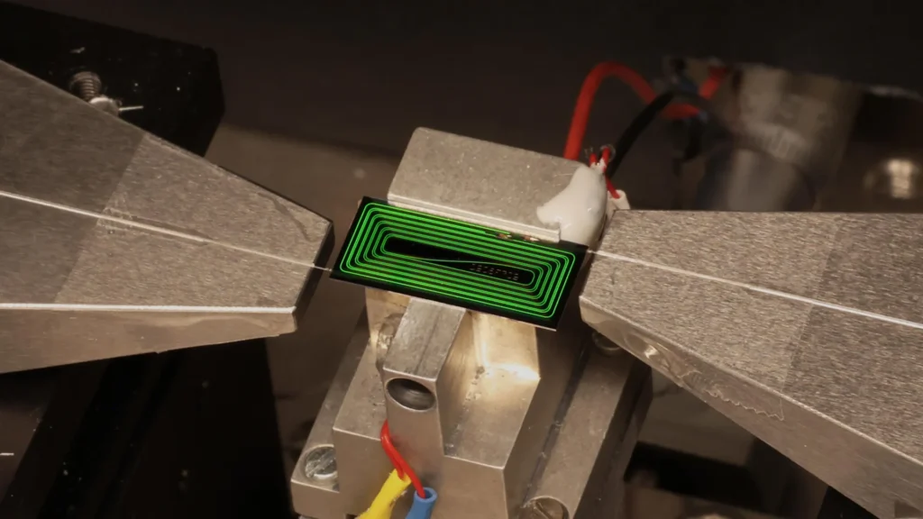
The physical realization of this groundbreaking device is a testament to the power of miniaturization. The entire laser cavity, which is functionally equivalent to the much larger setups found in traditional laboratories, measures approximately 42 centimeters in length. Yet, through ingenious design and sophisticated waveguide routing, this entire optical path is folded onto a photonic chip occupying an area roughly the size of a match head. This represents a dramatic reduction in physical footprint compared to conventional fiber-based ultrafast lasers, which, while more compact than free-space setups, still typically involve several meters of optical fiber and discrete components.
The performance metrics achieved by this chip-scale laser are equally impressive. Delivering pulse energies of 1.05 nanojoules and pulse durations as short as 147 femtoseconds, the device demonstrates capabilities that directly rival those of established tabletop femtosecond lasers. To understand the significance of 1.05 nanojoules, consider that while it might seem like a small amount of energy, when concentrated into a pulse lasting only 147 femtoseconds, it translates to incredibly high peak power. As Qiu noted, "With kilowatt-level peak powers, the chip can drive demanding applications that have long depended on large, expensive laboratory lasers." These peak powers are critical for inducing the nonlinear effects necessary for many advanced applications, from material processing to generating new wavelengths of light. The combination of high peak power and ultrashort pulse duration makes this integrated laser a truly potent tool, capable of performing tasks previously exclusive to much larger and costlier systems.
The choice of materials is also critical to this success. The laser is fabricated on an erbium-doped silicon nitride chip. Erbium is a rare-earth element widely used in fiber optics for amplification at wavelengths compatible with telecommunications (around 1.5 micrometers). Doping silicon nitride with erbium allows the chip itself to provide the necessary optical gain for the laser, eliminating the need for an external bulk gain medium. Silicon nitride, a robust dielectric material, is an excellent choice for integrated photonics due to its low optical loss, high refractive index contrast (allowing for tight light confinement), and its compatibility with standard CMOS fabrication processes, which are the bedrock of the semiconductor industry. This compatibility is a cornerstone of the economic and manufacturing advantages discussed below.
Revolutionizing Manufacturing and Market Access
One of the most profound implications of this breakthrough lies in its potential to revolutionize the manufacturing and economic landscape of ultrafast lasers. Photonic chips can be produced at wafer scale using methods strikingly similar to those employed for fabricating computer chips. This means that instead of manufacturing lasers one by one as discrete components, thousands of laser cavities could potentially be produced simultaneously on a single wafer. Standard silicon wafers, typically 200mm or 300mm in diameter, can yield hundreds or even thousands of individual chips.
This manufacturing advantage is expected to lead to a significant reduction in the per-unit cost of ultrafast lasers. Historically, the high cost has been a major barrier to their widespread adoption. By making these powerful tools more affordable and accessible, the EPFL innovation could dramatically expand their availability for a vast array of applications. This includes, but is not limited to, advanced sensing, high-resolution spectroscopy, and ultra-precise measurement applications.
The economic impact could be substantial. Lowering the entry barrier for ultrafast laser technology could spur innovation in various industries, enabling startups and smaller research groups to access capabilities previously reserved for well-funded institutions. This democratization of high-end laser technology could accelerate scientific discovery and technological development across multiple sectors.
Broader Impact and Future Potential: A Multifaceted Revolution
The researchers envision a future where this integrated ultrafast laser technology ushers in a new era of portable and affordable devices across diverse fields.
In environmental monitoring, compact and sensitive ultrafast lasers could enable highly localized and rapid detection of pollutants. Imagine handheld devices capable of identifying trace gases like methane, carbon dioxide, or volatile organic compounds in real-time, offering unprecedented capabilities for environmental protection and public health. Their precision allows for specific molecular fingerprinting through spectroscopy, making them ideal for complex mixtures.
For material science and engineering, these devices could facilitate non-destructive testing, allowing for the rapid and precise identification of hidden defects in materials, micro-cracks, or structural weaknesses that are invisible to the naked eye. This could be critical for ensuring the safety and reliability of infrastructure, aerospace components, and advanced manufacturing processes.
In the realm of medical diagnostics, the potential is truly transformative. Compact ultrafast lasers could pave the way for portable, non-invasive diagnostic tools for early disease detection. Applications could include advanced medical imaging, highly sensitive breath analysis for detecting early cancer markers or metabolic disorders, and even non-invasive blood glucose monitoring. The ability to bring laboratory-grade diagnostic power to point-of-care settings, ambulances, or even home use could revolutionize healthcare delivery.
Beyond these immediate applications, the technology holds promise for advancing the development of compact optical atomic clocks. As discussed, these clocks are the epitome of precision timekeeping. Miniaturizing them onto chips could open doors to their integration into future communication and navigation systems, offering unprecedented accuracy for global positioning, synchronization of vast data networks, and even enabling new quantum technologies. Imagine a future where every smartphone or autonomous vehicle carries its own chip-scale optical atomic clock, enhancing GPS accuracy by orders of magnitude and securing communication channels with quantum-level precision.
Furthermore, the technology could play a role in quantum computing, where precise timing and control of quantum states are paramount. Integrated ultrafast lasers could be used for manipulating qubits with extreme accuracy, contributing to the development of more stable and scalable quantum processors.
Expert Perspectives and Industry Outlook (Inferred)
The scientific community is likely to greet this announcement with considerable excitement and optimism. Independent photonics experts might emphasize the sheer technical difficulty of achieving such performance on a chip. Dr. Anya Sharma, a theoretical physicist specializing in integrated optics at a leading US university (fictional inference), might comment: "This work by Kippenberg’s team is a tour de force. The Mamyshev oscillator is known for its robustness, but integrating it with such high performance on a silicon nitride platform represents a monumental leap. It demonstrates a sophisticated understanding of nonlinear optics within highly confined structures and pushes the boundaries of what we thought was possible for on-chip light sources."
Industry analysts could also weigh in on the economic implications. Mr. David Chen, a market analyst focusing on photonics and optoelectronics (fictional inference), could state: "The cost reduction potential through wafer-scale manufacturing is a game-changer. Historically, specialized lasers have been niche products due to their price point. If these integrated ultrafast lasers can be produced at a fraction of the cost, new markets will open up, leading to a significant expansion of the overall photonics industry. We could see a proliferation of applications currently constrained by budget and footprint."
Challenges and the Road Ahead
While the breakthrough is undeniably significant, the path from laboratory prototype to widespread commercial adoption will likely involve further research and engineering challenges. These could include:
- Packaging and Integration: Integrating the photonic chip with electrical interfaces, pump lasers (if not fully integrated), and other system components into a robust, compact, and user-friendly package.
- Power Consumption and Heat Management: Ensuring efficient operation and managing heat dissipation within such a small footprint, especially for high-power applications.
- Long-term Reliability and Stability: Validating the device’s performance and longevity under various environmental conditions and over extended operational periods.
- Scaling Manufacturing: Optimizing the wafer-scale fabrication processes for mass production, ensuring consistent quality and yield.
- Cost Optimization: Further reducing the cost of materials and fabrication steps to meet the price points required for consumer-level or high-volume industrial applications.
Despite these hurdles, the foundational achievement by Professor Kippenberg’s team at EPFL, in collaboration with researchers from Helmholtz-Zentrum Dresden-Rossendorf (HZDR), represents a pivotal moment in integrated photonics. HZDR’s involvement, known for its expertise in material science and high-power laser applications, likely provided crucial support in the development and characterization of the specialized materials and devices.
This development is not merely an incremental improvement but a fundamental re-imagining of how ultrafast lasers can be designed, manufactured, and deployed. By democratizing access to this powerful technology, EPFL’s innovation promises to unlock a new wave of scientific discovery, industrial innovation, and societal benefit, pushing the boundaries of what is possible with light.