For decades, ultrafast lasers have stood as monumental pillars in modern optics, their fleeting pulses, lasting mere hundreds of femtoseconds—or quadrillionths of a second—underpinning an array of critical technologies. From the precision demands of advanced manufacturing and delicate eye surgery to the groundbreaking optical frequency combs, a Nobel Prize-winning innovation that now calibrates the world’s most accurate optical atomic clocks, their utility is undeniable. However, despite their profound importance and widespread application, these sophisticated instruments have largely remained cumbersome, prohibitively expensive systems, often demanding entire optical tables to house their complex components. This inherent bulkiness and cost have significantly limited their accessibility and integration into a broader spectrum of applications, confining their transformative power primarily to specialized laboratories and industrial settings. The pursuit of miniaturization, therefore, has been a long-standing "holy grail" within the integrated photonics community, promising to unlock unprecedented possibilities.
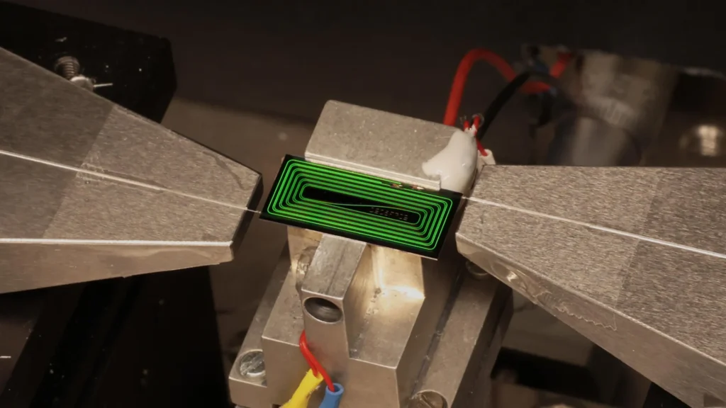
A significant paradigm shift is now on the horizon, following a groundbreaking achievement by researchers at EPFL (École Polytechnique Fédérale de Lausanne). Led by Professor Tobias J. Kippenberg, a team has successfully engineered the first integrated ultrafast laser capable of matching, and in some aspects even exceeding, the performance metrics of traditional tabletop femtosecond lasers. This monumental development, detailed in a recent publication in the prestigious journal Nature, describes a device that delivers impressive pulse energies of 1.05 nanojoules and pulse durations as short as 147 femtoseconds, all from a photonic chip that occupies an area roughly the size of a match head. This innovation represents a dramatic reduction in size and complexity, signaling a new era for ultrafast laser technology and its potential applications across numerous sectors.
A Legacy of Precision: The Evolution of Ultrafast Lasers
The journey of ultrafast lasers is marked by decades of relentless innovation, fundamentally altering our understanding and manipulation of light. The concept of generating extremely short pulses of light gained significant traction in the 1960s with the advent of mode-locking techniques, which allowed for the synchronization of multiple laser modes to produce a single, high-intensity pulse. Early systems, however, struggled with power limitations; increasing pulse energy often led to material damage within the laser components due to the extremely high peak powers involved.
A pivotal breakthrough arrived in the mid-1980s with the development of Chirped Pulse Amplification (CPA) by Donna Strickland and Gérard Mourou, a technology for which they were awarded the Nobel Prize in Physics in 2018. CPA works by stretching a short, low-energy pulse in time, amplifying it, and then recompressing it back to its original short duration. This ingenious method reduces the peak power during amplification, preventing optical damage and allowing for the generation of pulses with unprecedented peak intensities. CPA-based systems rapidly became the backbone of high-power ultrafast laser research and applications, driving advancements in fields from micromachining to fundamental plasma physics.
Concurrently, the development of optical frequency combs, pioneered by John L. Hall and Theodor W. Hänsch (who shared the Nobel Prize in Physics in 2005), further solidified the importance of ultrafast lasers in precision metrology. Frequency combs, essentially highly stable, broadband light sources generated by ultrafast lasers, act as "rulers" for light, enabling the most accurate measurements of optical frequencies and underpinning the next generation of atomic clocks. These advancements, while revolutionary, invariably relied on large, complex, and costly free-space optical setups or fiber-based systems, which, while more compact than earlier iterations, still presented significant barriers to widespread adoption and integration. The average cost for a high-performance femtosecond laser system can range from tens of thousands to several hundred thousand US dollars, alongside the substantial space requirements.
The Promise of Integrated Photonics: Shrinking the Optical World
Integrated photonics represents the optical analogue to microelectronics, aiming to manipulate and process light signals on a chip using microscopic structures called waveguides. Just as electronic chips have revolutionized computing by integrating millions of transistors onto a silicon wafer, photonic chips seek to miniaturize and integrate complex optical functionalities. These chips are fabricated using techniques similar to those employed for computer chips, leveraging semiconductor manufacturing processes to etch waveguides and other optical components onto a wafer.
The field has seen tremendous success, particularly in telecommunications, where photonic integrated circuits (PICs) are crucial for high-speed data transmission and optical networking. They have enabled the miniaturization of components like transceivers, modulators, and switches, leading to higher bandwidth, lower power consumption, and reduced costs. However, integrating active laser sources, especially high-performance ultrafast lasers, onto these chips has presented formidable challenges. The inherent requirements of ultrafast lasers—generating high peak powers, managing significant nonlinear optical effects, and maintaining precise pulse characteristics—are notoriously difficult to reconcile with the confined spaces and material limitations of chip-scale platforms. For decades, the notion of a high-pulse-energy femtosecond laser on a chip remained a distant aspiration, often referred to as a "holy grail" due to the immense technical hurdles involved.
Professor Kippenberg, a leading figure in integrated photonics and quantum optics, encapsulates this long-standing ambition, stating, "For more than twenty years, a high-pulse-energy femtosecond laser on chip was widely regarded as a holy grail of integrated photonics. Our result shows that it is not only possible, but that it can be achieved with a surprisingly elegant architecture that the integrated-photonics community had overlooked." This statement underscores not only the significance of the achievement but also the unexpected path taken to reach it.
An Overlooked Design Delivers: The Mamyshev Oscillator’s Triumph
The core of the EPFL breakthrough lies in the judicious selection and ingenious adaptation of a laser architecture known as the Mamyshev oscillator. This design, while known in the broader laser community, had received relatively little attention within the specific context of integrated photonics. The researchers’ decision to revisit and optimize this particular configuration proved to be a stroke of genius, offering a solution to many of the inherent challenges of chip-scale ultrafast laser generation.
At its heart, the Mamyshev oscillator system incorporates a nonlinear waveguide strategically placed between two distinct optical filters. Each filter is designed to transmit a different, specific portion of the light spectrum. The operational principle is elegantly simple yet remarkably effective: as an intense laser pulse propagates through the nonlinear waveguide, it undergoes a process called spectral broadening, expanding its range of colors. Only a part of this spectrally broadened pulse possesses the necessary characteristics to successfully pass through both optical filters, allowing it to continue circulating within the laser cavity. Weaker light, conversely, does not broaden sufficiently and is subsequently blocked by the filters, effectively being removed from the laser cycle. This selective filtering mechanism ensures that only high-intensity, spectrally broadened pulses are sustained, naturally leading to the generation of ultrafast pulses.
Zheru Qiu, a co-leading author of the paper, elaborated on the advantages of this design: "This design is especially attractive because it does not require any component that is difficult to make on this erbium-doped silicon nitride chip." This highlights a critical aspect of integrated photonics: the ease of fabrication. Complex structures or exotic materials often translate to higher manufacturing costs and reduced yields. The Mamyshev oscillator’s compatibility with standard silicon nitride fabrication processes, particularly when doped with erbium for optical gain, was a key enabler. Silicon nitride is a preferred material for high-performance integrated photonics due to its low optical loss, high refractive index contrast, and strong optical nonlinearity, making it ideal for guiding and manipulating light within micron-scale structures.
Furthermore, Qiu points out another major advantage: the Mamyshev oscillator’s inherent robustness against nonlinear effects. Photonic chips, by their very nature, confine light to extremely small waveguides. This tight confinement dramatically enhances the interaction between light and the material, leading to pronounced nonlinear optical phenomena. While these nonlinearities are essential for pulse generation in many ultrafast laser architectures, they can also introduce instabilities, distort pulses, and even lead to laser breakdown if not carefully managed. The Mamyshev oscillator, however, is far less susceptible to these detrimental effects, making it exceptionally well-suited for the highly nonlinear environment of integrated photonic devices. This intrinsic stability simplifies the design and operation of the chip-scale laser, a crucial factor for practical applications.
Miniaturization and Manufacturing: A New Era of Accessibility
The sheer scale of miniaturization achieved is astounding. The entire laser cavity, which is functionally equivalent to components that would typically span significant portions of an optical bench, measures approximately 42 centimeters in effective length. Yet, through clever optical folding techniques, this entire cavity is integrated onto a chip occupying an area no larger than a match head. This represents a dramatic reduction in physical footprint compared to conventional fiber-based ultrafast lasers, which, while more compact than free-space systems, still require substantial volumes.
Beyond the immediate size reduction, the manufacturing implications are profound. Photonic chips, including the erbium-doped silicon nitride platform used in this research, can be manufactured at wafer scale. This means that, similar to the production of computer chips, hundreds, or even more than 1,000, individual laser cavities could potentially be produced simultaneously on a single wafer. This parallel manufacturing capability stands to significantly drive down the per-unit cost of ultrafast lasers. Current tabletop femtosecond lasers are often bespoke or low-volume productions, contributing to their high price tags. Wafer-scale manufacturing promises to democratize access to these powerful tools, expanding their availability far beyond specialized research institutions and large industrial facilities.
Unlocking New Horizons: Broad Impact and Implications
The miniaturization and cost reduction brought about by this integrated ultrafast laser technology have the potential to spark a revolution across numerous scientific, industrial, and consumer sectors. The ability to generate kilowatt-level peak powers from a chip-scale device means it can drive demanding applications that have long been the exclusive domain of large, expensive laboratory lasers.
Precision Manufacturing and Industrial Applications: Ultrafast lasers are indispensable for advanced materials processing, including micromachining, drilling, and cutting with extreme precision and minimal heat-affected zones. Chip-scale ultrafast lasers could enable more compact, portable, and cost-effective laser processing tools, facilitating their integration into smaller production lines, field repair kits, or even novel additive manufacturing systems. The ability to identify hidden defects in materials, as mentioned by the researchers, could also be dramatically enhanced through portable inspection devices.
Medical Diagnostics and Treatment: In medicine, femtosecond lasers are already used in highly precise procedures like LASIK eye surgery, where their ultrashort pulses minimize collateral tissue damage. Miniaturized ultrafast lasers could lead to the development of portable diagnostic tools for real-time medical imaging (e.g., optical coherence tomography, multiphoton microscopy) that could be used in clinics, ambulances, or remote areas, potentially revolutionizing point-of-care diagnostics and minimally invasive surgery.
Environmental Sensing and Monitoring: The precise spectroscopic capabilities of ultrafast lasers make them ideal for detecting trace amounts of environmental pollutants. Chip-scale devices could enable the deployment of vast networks of affordable, compact sensors for continuous monitoring of air and water quality, hazardous gases, or even biological agents in various environments, from urban centers to remote industrial sites.
Metrology, Timing, and Navigation: The link between ultrafast lasers and optical frequency combs is critical for the world’s most accurate timekeeping. Compact optical atomic clocks, leveraging these integrated lasers, could surpass the precision of current microwave-based atomic clocks, leading to unprecedented accuracy in global navigation satellite systems (GNSS) like GPS, enabling next-generation communications, and supporting fundamental research in physics, such as searches for dark matter or variations in fundamental constants. The potential for enhancing GPS accuracy by orders of magnitude could have significant implications for autonomous vehicles, precision agriculture, and defense applications.
Scientific Research and Fundamental Physics: Accessible, high-performance ultrafast lasers will empower a new generation of researchers. They will provide more affordable tools for spectroscopy, nonlinear optics experiments, and studies of ultrafast phenomena in materials science, chemistry, and biology, potentially leading to unforeseen discoveries.
Challenges and the Road Ahead
While the EPFL breakthrough is monumental, the journey from laboratory demonstration to widespread commercial adoption will involve further research and development. Key challenges include optimizing power output for even more demanding industrial applications, enhancing the long-term reliability and robustness of the chip-scale lasers for real-world environments, and developing packaging solutions that can withstand varying temperatures and vibrations. Further integration of other optical components, such as detectors and modulators, onto the same chip would also enhance functionality and compactness.
The work, involving researchers from the EPFL Institute of Electrical and Microengineering and Helmholtz-Zentrum Dresden-Rossendorf (HZDR), represents a culmination of expertise across material science, photonics engineering, and laser physics. The scientific community’s initial reactions are overwhelmingly positive, recognizing the profound implications of moving such a powerful tool from large optical tables to the palm of one’s hand. Industry observers anticipate a significant disruption to the existing ultrafast laser market, with the potential for new market segments to emerge driven by the accessibility and affordability of these chip-scale devices.
In conclusion, the EPFL team’s achievement marks a pivotal moment in the history of optics and photonics. By shrinking the formidable power of ultrafast lasers onto a silicon nitride chip, they have not only overcome a long-standing technical barrier but have also opened the floodgates for an explosion of new applications across medicine, manufacturing, environmental monitoring, and fundamental science. This breakthrough promises to democratize access to one of modern optics’ most powerful tools, ushering in an era where the precision and speed of femtosecond lasers become ubiquitous, transforming countless aspects of our technological landscape and scientific endeavor.