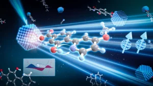
In a breakthrough that bridges the gap between fundamental quantum physics and scalable materials science, researchers at the Massachusetts Institute of Technology (MIT) have identified a new class of "moiré crystals" wherein electrons behave as though they are navigating a four-dimensional spatial environment. This phenomenon, which allows electrons to seemingly "teleport" through a synthetic fourth dimension perpendicular to our perceivable three-dimensional reality, was facilitated by a novel chemical synthesis technique that overcomes a decade-long bottleneck in the production of quantum materials. The study, published recently in the journal Nature, marks a significant shift from the laborious, manual assembly of two-dimensional sheets to a scalable, high-quality production method that could pave the way for next-generation electronic and superconducting applications.
The discovery centers on the strange behavior of electrons within moiré superlattices—complex interference patterns created when layers of atoms are stacked with slight misalignments or differing periodicities. While traditional electronics rely on the flow of electrons through three dimensions, the MIT team found that in these specific crystals, the electrons act as if they are moving through an emergent "superspace." This behavior is not a property of the electrons themselves, but rather a result of the unique structural environment provided by the moiré crystal, which effectively simulates a higher-dimensional landscape.
The Evolution of Moiré Materials: A Decade of Discovery
The field of moiré materials has its roots in the study of graphene, a single layer of carbon atoms arranged in a hexagonal lattice. For over a decade, physicists have manipulated these materials to unlock exotic quantum states. The timeline of these discoveries highlights MIT’s central role in this scientific frontier:
- 2014: Researchers in the labs of Professors Pablo Jarillo-Herrero and Raymond Ashoori discovered that electrons in moiré materials composed of graphene and boron nitride inhabit a quantum fractal structure known as "Hofstadter’s butterfly." This proved that moiré patterns could fundamentally alter electronic energy levels.
- 2018: A landmark study from the Jarillo-Herrero lab revealed that "magic-angle" twisted bilayer graphene could exhibit unconventional superconductivity. By twisting two sheets of graphene to exactly 1.1 degrees, the material could conduct electricity with zero resistance, becoming one of the strongest known superconductors relative to its electron density.
- 2024: Associate Professor Long Ju and his team demonstrated that moiré materials could cause electrons to split into fractional pieces, a phenomenon previously seen only under extreme magnetic fields. This discovery suggested that moiré structures could democratize access to advanced quantum states.
- 2025: The broader scientific community recognized the importance of large-scale superconducting circuits and quantum tunneling, themes central to the 2025 Nobel Prize in Physics. The current MIT study builds upon this momentum by introducing a scalable method to produce these materials and revealing their higher-dimensional properties.
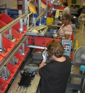
Until now, the primary challenge facing this field was the "materials bottleneck." Creating moiré devices required students and postdocs to manually peel 2D layers from bulk crystals using adhesive tape—a process colloquially known as the "Scotch tape method." These layers were then painstakingly aligned and stacked under microscopes. While effective for laboratory proofs-of-concept, this method was non-scalable and prone to human error.
A Breakthrough in Chemical Synthesis and Scalability
The research team, led by corresponding author Joe Checkelsky, a professor of physics at MIT, and co-lead authors Kevin Nuckolls and Nisarga Paul, sought a more industrial-ready approach. Instead of manual stacking, they developed a chemical synthesis route that allows Mother Nature to grow moiré crystals with built-in superlattices.
In this new method, the researchers grow bulk crystals where the moiré pattern is repeated throughout every layer of the material. This is analogous to moving from a single hand-drawn diagram to a printed library. While previous methods produced individual, fragile stacks, Checkelsky’s team can now generate thousands of high-quality moiré layers simultaneously. These "moiré crystals" are nearly perfect in their atomic alignment and highly reproducible, addressing the consistency issues that have plagued the field for years.
"It feels incredible for our team to have made this materials discovery," stated Kevin Nuckolls, a Pappalardo postdoc in physics at MIT. "Nature is by far the best at assembling moiré materials when given the right tools. This offers a proof-of-concept for a scalable route to using these materials in electronics."
Navigating the 4D Superspace: Quantum Tunneling and Shadows
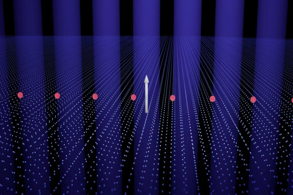
The most striking aspect of the study is the discovery of the synthetic fourth dimension. In physics, dimensions are defined by the degrees of freedom available to a particle. While we perceive only three spatial dimensions, the mathematical equations governing electron dynamics in these new crystals require a four-dimensional framework.
This 4D behavior is facilitated by "quantum tunneling." In the macroscopic world, a ball at the bottom of a valley stays there unless pushed. In the quantum world, a particle can "tunnel" through a barrier, appearing on the other side as if by magic. In moiré crystals, the interference between two competing lattices creates a "superspace" lattice. When electrons tunnel within this environment, they behave as though they have entered a fourth dimension perpendicular to the 3D plane.
"Mathematically, the equations describing the electron dynamics in these crystals are four-dimensional," explained co-lead author Nisarga Paul. "The electrons propagate in the synthetic dimension just as they do in our world’s three physical dimensions."
To verify this, the team conducted experiments at the National High Magnetic Field Laboratory. By applying intense magnetic fields, they observed "quantum oscillations"—periodic fluctuations in the material’s electronic properties. These oscillations served as "fingerprints" or "shadows" of the 4D landscape. By analyzing these 3D silhouettes from various angles, the researchers were able to reconstruct the 4D environment that guides the electrons.
Data Analysis and Experimental Methodology
The research involved a multi-institutional collaboration including Harvard University, Toho University, and the National High Magnetic Field Laboratory. Key data points from the study include:
- Lattice Interference: The researchers utilized two different 2D materials that were structurally similar but not identical. This ensured a permanent misalignment that generated a consistent moiré superlattice across the entire bulk crystal.
- Quantum Oscillation Frequency: Under high magnetic fields, the frequency of electronic oscillations matched the theoretical predictions for a 4D superspace lattice, rather than a standard 3D or 2D lattice.
- Reproducibility Rates: Unlike the manual stacking method, which often results in varied twist angles and performance, the chemically grown moiré crystals showed a near 100% success rate in maintaining the desired superlattice structure across multiple batches.
This data suggests that the "synthetic dimension" is more than just a mathematical curiosity; it is a functional reality for the electrons. Even if the fourth dimension is technically fictitious in a physical sense, the material’s properties—such as conductivity and magnetic response—react as if the dimension were real.
Broader Impact and Future Implications
The implications of this discovery extend far beyond the laboratory. By providing a scalable way to produce materials that simulate higher dimensions, MIT researchers have opened the door to realizing theoretical predictions that were previously considered unreachable.
High-Dimensional Superconductivity
One of the most anticipated applications is the study of higher-dimensional superconductivity. Current superconductors are often limited by the constraints of 2D or 3D space. Materials that allow electrons to interact across synthetic dimensions could potentially lead to superconductors that operate at higher temperatures or with greater stability, revolutionizing energy grids and transportation.
Topological Properties and Quantum Computing
The study also provides a platform for exploring higher-dimensional topological properties. In quantum computing, topological insulators are highly sought after because they can protect quantum information from environmental "noise." Synthetic dimensions could allow for the creation of more robust topological states, facilitating the development of more reliable quantum processors.
Next-Generation Electronics
The scalability of the chemical synthesis method suggests that moiré crystals could eventually be integrated into standard semiconductor manufacturing. If the "teleportation" of electrons through synthetic dimensions can be controlled, it could lead to transistors and circuits that are faster and more energy-efficient than current silicon-based technology.
Conclusion
The research led by Professor Joe Checkelsky and his colleagues at MIT represents a pivotal moment in condensed matter physics. By combining innovative chemical synthesis with advanced quantum theory, the team has not only solved a major material science hurdle but has also expanded the spatial horizon of electronic motion.
"There are long-standing theoretical predictions for higher-dimensional conductors and superconductors," Checkelsky noted. "Materials of this type may offer a new platform to examine these experimentally in the laboratory."
The study was supported by an array of prestigious institutions, including the Gordon and Betty Moore Foundation, the U.S. Department of Energy, and the National Science Foundation. As the scientific community continues to digest these findings, the focus will likely shift toward practical applications, moving the "synthetic fourth dimension" from the realm of physics theory into the hardware of the future. While many obstacles remain before these materials appear in consumer electronics, the path from "Scotch tape" to "scalable crystals" has now been clearly illuminated.