The pervasive issue of overheating, a familiar nuisance for laptop users, extends its critical impact to the global infrastructure of computer servers and vast data centers. As computer chips continue their relentless march towards greater compactness and power, the challenge of effective heat management escalates, threatening to become a fundamental bottleneck for technological progress. This escalating thermal hurdle necessitates a deeper, more granular understanding of heat dynamics within microelectronic components, particularly in the complex, multilayered devices that underpin our modern digital world. Traditional methods for measuring heat flow have largely struggled with the intricacies of such architectures, often failing to provide the precision needed at the micro and nanometer scales.
The Overheating Challenge: A Bottleneck for Modern Technology
The relentless pursuit of faster, more powerful computing has driven semiconductor manufacturers to pack ever-increasing numbers of transistors into smaller silicon footprints. This adherence to Moore’s Law, while enabling exponential growth in processing power, simultaneously amplifies the challenge of heat dissipation. Every operation performed by these miniature electronic switches generates heat, and as transistors become denser and operate at higher frequencies, the amount of heat produced per unit area skyrockets.
This thermal burden manifests in several critical ways. For consumers, it translates into laptops that throttle performance to prevent damage, or mobile devices that become uncomfortably warm. For the industrial backbone of the internet, data centers face an immense energy challenge. Estimates suggest that cooling systems can account for a substantial portion of a data center’s total energy consumption, often ranging from 30% to 50% of its operational energy budget. Globally, data centers already consume an estimated 1-2% of the world’s electricity, a figure projected to rise dramatically with the proliferation of cloud computing, artificial intelligence (AI), and advanced analytics. Inefficient thermal management not only inflates operational costs but also leads to reduced component lifespan, decreased reliability, and the necessity for more frequent hardware upgrades, collectively impacting economic efficiency and environmental sustainability.
The physics behind this problem is rooted in Joule heating, where the resistance to current flow within the tiny wires and transistors converts electrical energy into heat. While engineers have developed various thermal management solutions—from sophisticated heatsinks and thermal pastes to advanced liquid cooling systems—these often address the macroscopic removal of heat. The real challenge lies in understanding and managing heat at the micro-scale, within the intricate layers of the chip itself, where localized "hotspots" can emerge and compromise performance long before the entire device reaches critical temperatures. The ability to precisely track how heat moves through these minute, multilayered structures is thus paramount for unlocking the next generation of high-performance electronics.
Traditional Methods Fall Short: The Need for Micro-Scale Precision
For years, researchers have employed a variety of techniques to measure and model heat flow in materials. These include optical methods like Time Domain Thermal Reflectance (TDTR) and imaging techniques such as infrared (IR) cameras. While valuable, these methods possess inherent limitations when confronted with the complexity of modern device architectures.
Time Domain Thermal Reflectance, for instance, relies on optical probes to detect temperature changes on a material’s surface. As MIT Associate Professor Jeehwan Kim explains, "Because that technique uses optics, it doesn’t allow you to study different layers. Real devices have five or more layers. It also only provides an overall signal, and that makes it hard to see thermal transport happening in layers buried under the surface." This limitation is critical because heat transfer often involves complex interactions across multiple interfaces and within different material layers, each possessing distinct thermal properties. An average signal fails to capture the localized phenomena that dictate a device’s ultimate thermal performance.
Similarly, infrared cameras, while excellent for visualizing temperature distributions across larger surfaces, often lack the spatial resolution and temporal precision required to capture the rapid, tiny thermal changes occurring within compact, high-frequency chips. The speed at which heat dissipates or propagates at the nanoscale is extraordinarily fast, often on the picosecond to nanosecond scale, making it challenging for slower, macroscopic imaging techniques to provide meaningful data. The inability of these conventional methods to "get down to the micro- or nanometer scale," as articulated by Associate Professor Mingda Li, has left a critical gap in the diagnostic toolkit for chip developers. This gap prevents them from precisely identifying the causes of local hotspots and designing devices with superior thermal performance.
A New Frontier in Thermal Metrology: X-rays Meet Lasers
Addressing these profound limitations, a team of researchers from MIT has developed a novel and highly precise method to study heat transport within multilayered materials. Published in Nature Communications, their technique marries the penetrating power of X-rays with the localized heating capabilities of ultrafast laser pulses, offering an unprecedented view into the thermal dynamics of advanced electronic devices.
The core innovation lies in leveraging an emerging analysis technique that utilizes both electron pulses and ultrafast X-rays. This approach capitalizes on the significant advancements in X-ray source technology over recent years. As co-lead author Thanh Nguyen PhD ’24 explains, "Over the last few years, researchers have developed what is basically the brightest X-ray source in the world. That allows you to focus an X-ray beam and get incredibly fine spatial resolution." Such ultra-bright X-ray sources, typically found at advanced synchrotron facilities like the Advanced Photon Source (APS) at Argonne National Laboratory or X-ray free-electron lasers (XFELs) like SLAC’s Linac Coherent Light Source (LCLS), can deliver X-ray beams with exquisite spatial and temporal coherence. These X-rays are energetic enough to penetrate multiple layers of a material without significant attenuation, allowing researchers to probe subsurface structures.
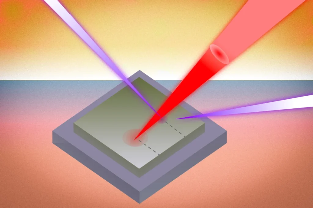
Simultaneously, the technique employs laser pulses to deliver highly localized and transient heat to the sample. These laser pulses induce rapid, precise temperature changes within specific regions of the material. As the material heats and cools, its atomic lattice expands and contracts, leading to subtle changes in its crystal structure. The X-rays, passing through these heated regions, interact with the atomic lattice and undergo diffraction. By meticulously measuring these diffraction patterns in real-time as the heat propagates, researchers can infer the temperature distribution and strain within each layer.
Co-lead author Chuliang Fu elaborates on the advantage: "Using previous measurement techniques, in real devices, you couldn’t resolve what happens on one layer versus another, so you’d just measure the average. X-rays can clearly show how heat propagates across the interface through their diffraction." This ability to differentiate thermal events layer-by-layer is a game-changer, providing specific insights into how heat carriers—primarily phonons (quantized lattice vibrations)—move and interact within the complex heterostructures of modern chips. The combined approach of laser-induced heating and ultrafast X-ray diffraction thus offers a clearer, more resolved view of how a material moves heat, both spatially and temporally.
Unveiling Hidden Flaws: Precision at the Micron Scale
To demonstrate the efficacy of their new method, the MIT team applied it to a test device constructed from gallium nitride (GaN) grown on a silicon substrate. Gallium nitride is a wide-bandgap semiconductor material that has garnered significant interest in the electronics industry due to its superior properties for high-power, high-frequency applications, including transistors and flexible electronics. Its theoretical thermal conductivity is high, making it a promising candidate for efficient heat dissipation. However, its practical thermal performance has often been observed to deteriorate due to defects introduced during the manufacturing process, particularly at the interface between the GaN and the silicon substrate.
The precision of the MIT technique allowed the researchers to quantify the impact of a single micron-scale defect within this GaN-on-silicon device. Their findings were striking: they observed a fourfold reduction in the material’s ability to transfer heat at the location of a specific "wrinkle defect." Furthermore, the defect caused heat to spread unevenly, exhibiting anisotropic thermal transport – moving more easily in one direction than another. They also measured a 25 percent overall drop in heat dissipation across the materials due to processing-induced imperfections.
These results are particularly significant because conventional thermal models often assume ideal, defect-free crystals. As Professor Li notes, "When people model heat dissipation, they model perfect crystals without defects. But these types of large wrinkle defects are very common in 2D materials. People never even knew how much heat is blocked by these wrinkles. Those are things we can now directly observe with this technique." This direct experimental evidence of how subtle, micron-scale manufacturing imperfections drastically impede thermal flow provides critical data for improving material growth and device fabrication processes. It bridges the gap between theoretical idealizations and the complex realities of semiconductor manufacturing.
Broader Implications: Powering the Next Generation of Electronics
The implications of this breakthrough extend far beyond academic research, promising to catalyze significant advancements across a spectrum of technologies. The ability to precisely diagnose thermal bottlenecks at the micro-scale is crucial for developing more power-dense and efficient electronic systems.
For the burgeoning field of artificial intelligence (AI), which demands immense computational power and thus generates substantial heat, this technique offers a pathway to design more efficient AI accelerators. These specialized chips are the backbone of machine learning algorithms, and their performance is often limited by their ability to dissipate heat. Similarly, in the realm of wearable electronics, where device size and battery life are paramount, better thermal management can lead to smaller, lighter, and more energy-efficient gadgets. In clean energy systems, such as power converters for electric vehicles or solar inverters, high-efficiency power electronics are critical. Overheating in these components reduces efficiency and lifespan, making advanced thermal design a key enabler for wider adoption.
Professor Li emphasizes the urgency: "Chip developers need devices that can handle heat. I think overheating has become the real bottleneck in device performance." He further explains that the ability to "study the heat carriers and understand exactly what causes failure, in order to avoid local hotspots and design better devices" is a fundamental step toward overcoming this bottleneck. Understanding the behavior of phonons—the primary heat carriers in semiconductors—at interfaces and around defects is essential for engineering materials with tailored thermal properties. This technique provides the means to directly observe these behaviors.
Industry Recognition and Future Outlook
The impact of this research is already resonating within the semiconductor industry. The article reveals that a "leading semiconductor industry consortium" has already reached out to collaborate with the MIT team, seeking to apply this novel measurement technique to study various types of chips. This immediate industry interest underscores the critical need for such diagnostic tools and the recognition of the technique’s potential to accelerate product development.
Associate Professor Kim highlights the significance of this industry interest: "We can now pass a current and shine an X-ray on a device and see how the heat dissipates at a very small scale. That’s something the industry has been longing for." The ability to conduct in-situ measurements—observing heat dissipation while a device is actively operating and carrying current—provides invaluable insights that static measurements cannot capture. This comprehensive view will allow engineers to optimize not just material selection, but also device geometry and layout, which are crucial for effective thermal design. "Even with the same type of materials, the geometry and how the materials are laid out is quite complicated, so it will show us how those differences impact thermal flow by providing direct experimental measurements," Kim adds.
Looking ahead, the researchers believe their approach is broadly applicable to a wide array of materials and device architectures, not limited to GaN-on-silicon. It could be used to investigate thermal transport in other wide-bandgap semiconductors like silicon carbide (SiC), emerging 2D materials, quantum computing components, and advanced packaging technologies. By providing a clear, experimental understanding of thermal performance at the micro-scale, this MIT innovation stands to empower scientists and engineers to design chips that are not only more powerful but also more reliable, energy-efficient, and sustainable, paving the way for the next wave of technological breakthroughs.
The collaborative effort behind this groundbreaking work involved a diverse team of researchers. Joining Professors Mingda Li and Jeehwan Kim as co-corresponding authors were co-lead authors Thanh Nguyen PhD ’24 and MIT postdoc Chuliang Fu. The extensive list of contributors includes PhD candidate Mouyang Cheng; Abhijatmedhi Chotrattanapituk ’21, SM ’26; Denisse Córdova Carrizales SM ’26; Eunbi Rha SM ’26; Tyra Espedal ’26; Buxuan Li PhD ’24; Shivam Kajale SM ’23, PhD ’26; Tongtong Liu PhD ’23; Kuan Qiao PhD ’22; University of Texas at Austin Assistant Professor Zhantao Chen SM ’18, PhD ’22; Argonne National Laboratory researchers Kumar Neeraj, Donald Walko, and Haidan Wen; MIT Principal Research Scientist Svetlana Boriskina; and MIT Associate Professor Deblina Sarkar. The research received vital support from the U.S. Department of Energy, the U.S. National Science Foundation, and the MIT School of Engineering Distinguished Energy Efficiency Fellowship.