In the intricate realm of quantum materials, where the rules of classical physics give way to quantum phenomena, the organization of electrons often defies simple, uniform descriptions. Rather than forming smooth, homogeneous states, electronic order frequently manifests as complex, spatially varying patterns. Among the most widely studied of these phenomena is the charge density wave (CDW), a collective electronic state where electrons spontaneously arrange themselves into a repeating, periodic pattern, akin to a standing wave, at sufficiently low temperatures. While CDWs have been a subject of intense research for decades, a significant challenge has persisted: directly observing how their strength, known as amplitude, and their spatial coherence – how uniformly and extensively these patterns spread – evolve during a phase transition has remained elusive. This lack of direct observation has hindered a complete understanding of the fundamental mechanisms governing these fascinating electronic states.
A groundbreaking study led by Professor Yongsoo Yang of the Department of Physics at the Korea Advanced Institute of Science and Technology (KAIST), in collaboration with Professors SungBin Lee, Heejun Yang, and Yeongkwan Kim from KAIST, and a team of collaborators at Stanford University, has now achieved a monumental breakthrough in this field. For the first time, these researchers have directly visualized the spatial evolution of the charge density wave order’s amplitude within a quantum material, offering an unprecedented window into the complex dynamics of electronic organization at the nanoscale. This pioneering work provides empirical data that challenges long-held assumptions and opens new avenues for exploring the foundational principles of quantum matter.
The Enduring Enigma of Charge Density Waves
Quantum materials are a class of substances where quantum mechanical effects, such as electron-electron interactions and electron-lattice coupling, dictate their macroscopic properties. These materials often exhibit exotic behaviors, including superconductivity, colossal magnetoresistance, and topological states, which hold immense promise for future technologies. Understanding the various forms of electronic order within these materials is paramount to harnessing their potential.
Charge density waves are a quintessential example of such electronic order. They arise when the electrons in a material, typically at low temperatures, spontaneously rearrange themselves into a periodic modulation of charge density. This modulation is accompanied by a slight distortion of the crystal lattice, known as a Peierls distortion. The concept of CDWs dates back to the theoretical work of Rudolf Peierls in the 1950s, predicting that a one-dimensional metal would be unstable to such a distortion. Since then, CDWs have been observed in a wide range of materials, including transition metal dichalcogenides (e.g., NbSe₂, TaS₂), high-temperature superconductors, and other exotic compounds.
The importance of CDWs extends beyond their intrinsic interest. They frequently compete or coexist with other fundamental electronic states, such as superconductivity and magnetism. For instance, in many high-temperature superconducting cuprates, CDW order has been observed, and its interaction with superconductivity is a subject of intense debate. Understanding the formation and evolution of CDWs is thus crucial for deciphering the intricate interplay of forces that govern the properties of these complex materials and for potentially designing new materials with enhanced functionalities.
Despite decades of research, much of our knowledge about CDWs has been derived from indirect experimental techniques, primarily X-ray or electron diffraction. These methods provide ensemble-averaged information about the periodicity and presence of CDW order across a macroscopic sample. While invaluable, they offer limited insight into the local variations in CDW strength or how these ordered regions connect and interact across space. Scanning probe microscopy techniques, such as scanning tunneling microscopy (STM), can provide atomic-scale spatial information, but they are typically surface-sensitive and may not fully capture the bulk behavior or the dynamic evolution during phase transitions, particularly across a range of temperatures. The direct visualization of CDW amplitude and spatial coherence during a phase transition, therefore, represented a critical missing piece in the puzzle of quantum materials.
A Novel Nanoscale Imaging Approach: 4D-STEM at Cryogenic Temperatures
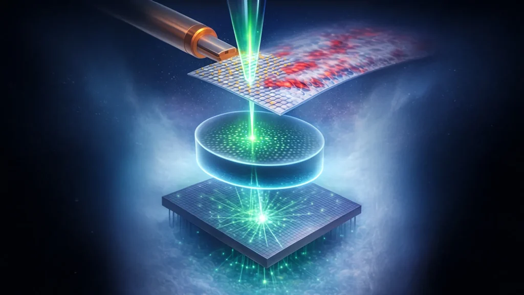
To overcome these long-standing experimental limitations, the KAIST-Stanford research team employed an exceptionally advanced experimental setup: a liquid-helium-cooled electron microscope integrated with four-dimensional scanning transmission electron microscopy (4D-STEM). This sophisticated instrumentation was key to their success.
The liquid-helium-cooled electron microscope allows researchers to maintain the sample at extremely low temperatures, near -253°C (approximately 20 Kelvin). This cryogenic capability is essential because CDWs, like many other collective electronic states, typically form and are stable only at very low temperatures. By precisely controlling the temperature, the team could induce and track the phase transition of the CDW, observing its formation, weakening, and eventual breakdown as the temperature was varied.
The heart of their imaging prowess lies in 4D-STEM. In traditional STEM, a focused electron beam scans across a sample, and a detector collects the scattered electrons to form an image. 4D-STEM elevates this by collecting a full two-dimensional diffraction pattern at every single pixel as the electron beam scans. This means that for each probe position (x, y), a 2D diffraction pattern (kx, ky) is recorded, resulting in a four-dimensional dataset (x, y, kx, ky). This rich dataset allows researchers to extract not only real-space images with atomic resolution but also detailed information about the local crystal structure, strain, and, critically, the local electronic order. By analyzing the intensity and shape of specific diffraction spots associated with the CDW, the researchers could quantitatively map the CDW amplitude and its spatial extent at the nanoscale.
This advanced setup offered several crucial advantages:
- Direct Visualization of Amplitude: Unlike diffraction, which provides an average signal, 4D-STEM allowed the team to map the local strength (amplitude) of the CDW order across the material.
- Nanoscale Spatial Resolution: The electron microscope could resolve structures as small as one hundred-thousandth the width of a human hair (on the order of a few nanometers), providing unprecedented detail into the spatial organization of the electronic patterns. For context, a typical human hair is about 100 micrometers wide, so this resolution is approximately 1 nanometer.
- Temperature-Dependent Dynamics: The cryogenic stage enabled the observation of how CDW order forms, evolves, and dissolves as the temperature changes, capturing the entire phase transition dynamically.
Professor Yang likened the process to "watching ice crystals form as water freezes, captured with extremely high magnification." However, in this case, the "ice crystals" were patterns of electrons arranging themselves at temperatures just above absolute zero, and the "magnification" was sufficient to resolve features at the scale of atomic arrangements. This meticulous experimental approach provided the first direct, spatially resolved view of a CDW’s amplitude and coherence evolution during a thermal phase transition.
Revealing Patchy Electronic Patterns and the Role of Strain
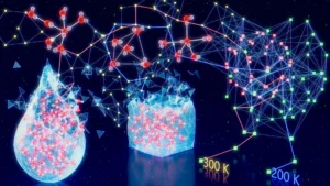
The high-resolution nanoscale maps generated by the 4D-STEM revealed several surprising and critical insights into the nature of CDW formation. Foremost among these was the discovery that electronic order does not spread uniformly or smoothly across the material. Instead, the images showed a distinct "patchy" character: some regions exhibited clear, strong, and well-defined CDW patterns, while adjacent areas showed little to no electronic order. This observation fundamentally challenges the classical view of phase transitions as homogeneous processes where order parameter emerges uniformly throughout the sample. The researchers vividly described this phenomenon as "resembling a lake where ice forms in scattered patches rather than covering the surface all at once." This spatial heterogeneity implies a more complex, localized nucleation and growth mechanism for electronic order than previously assumed.
Beyond the patchy distribution, the study uncovered a profound connection between these uneven patterns and subtle structural distortions within the crystal lattice. The team found that even "minute amounts of strain"—tiny, localized deformations in the atomic arrangement—were sufficient to significantly weaken the CDW amplitude in those regions. These strains were so small that they would be undetectable using conventional optical methods, highlighting the extreme sensitivity of these quantum electronic states to their atomic environment. This direct evidence confirms theoretical predictions about the strong coupling between the electronic system and the lattice in CDW materials. The finding underscores that even seemingly negligible imperfections or local variations in the crystal structure can play a crucial role in dictating where and how strongly electronic order can form, offering a powerful lever for potentially controlling these states.
Persistent Pockets and the Gradual Loss of Coherence
Another astonishing revelation from the study was the observation of small, isolated pockets of CDW order that persisted even above the material’s nominal transition temperature, the point where long-range order is typically expected to vanish completely. This finding further reinforces the idea that the phase transition is not a simple, abrupt, or uniform event. Instead of the electronic order disappearing all at once across the entire material, it appears to gradually lose its spatial coherence. Local regions of order can survive, albeit disconnected, in a "disordered" matrix, slowly dissolving as the temperature increases further. This suggests a more nuanced understanding of phase transitions in quantum materials, where local order can be far more robust and resilient than previously thought, even in the absence of macroscopic, long-range coherence.
A New Framework: Direct Measurement of CDW Amplitude Correlations
A pivotal technical achievement of this work is the first direct measurement of correlations in CDW amplitude. By quantitatively assessing how the strength of electronic order at one specific location relates to that at another, the researchers were able to precisely track and quantify how spatial coherence breaks down across the phase transition. This capability was previously unattainable with traditional diffraction techniques, which only provide averaged information, or with scanning probe methods, which, while offering local information, have struggled to provide a robust, temperature-dependent, and statistically significant measure of amplitude correlation in the bulk.
This direct measurement provides a new, powerful metric for characterizing phase transitions in quantum materials. It allows scientists to differentiate between a reduction in local order and a loss of global coherence, offering a more complete picture of how collective electronic states evolve. Understanding how coherence is established and lost is fundamental to the physics of emergent phenomena and critical for developing a comprehensive theoretical framework for these materials.
Broader Impact and Implications for Quantum Materials Science
This groundbreaking study by the KAIST-Stanford team has profound implications for the broader field of quantum materials science, extending far beyond the specific case of charge density waves.
-
Fundamental Understanding of Electronic Order: The direct visualization of patchy CDW formation, the strong influence of nanoscale strain, and the persistence of local order above the transition temperature fundamentally reshape our understanding of how collective electronic states form and evolve. It highlights the importance of spatial heterogeneity and local environmental factors in determining macroscopic material properties. This challenges the simplified, uniform picture often assumed in theoretical models and provides crucial experimental data to refine these models.
-
Guiding Material Design: By demonstrating the critical role of subtle lattice distortions (strain) in weakening CDW order, this research offers a new paradigm for materials design. If CDWs are detrimental to desired properties, such as high-temperature superconductivity (where CDWs often compete with the superconducting state), understanding how to control or suppress them through strain engineering could be a powerful tool. Conversely, if CDWs are desirable, identifying ways to stabilize them against strain could lead to more robust materials. This opens avenues for "strain engineering" quantum materials to tailor their electronic properties.
-
Interactions with Other Quantum States: Charge density waves rarely exist in isolation. They often interact intimately with other electronic orders, such as superconductivity, magnetism, and nematicity. By providing a spatially resolved view of CDW evolution, this study offers a new lens through which to investigate these complex interdependencies. For example, future studies could use this technique to map how CDW patches interact with superconducting regions or magnetic domains, potentially uncovering the mechanisms behind their competition or coexistence.
-
Advancing Experimental Techniques: The successful application of liquid-helium-cooled 4D-STEM sets a new benchmark for experimental capabilities in condensed matter physics. It demonstrates the immense power of combining advanced microscopy with cryogenic environments to probe the intricate details of quantum phenomena. This methodology can now be extended to study other complex electronic phases, such as spin density waves, orbital ordering, or even the nanoscale origins of unconventional superconductivity.
-
Path Towards Quantum Technologies: Ultimately, a deeper, more granular understanding of quantum materials is essential for realizing their technological potential. Whether it’s developing room-temperature superconductors, highly efficient quantum computers, or novel sensors, the ability to control and manipulate electronic order at the nanoscale is paramount. This research moves us closer to that goal by providing the fundamental knowledge and experimental tools needed to characterize and eventually engineer these exotic states of matter.
Dr. Yongsoo Yang articulated the profound significance of these findings: "Until now, the spatial coherence of charge density waves was largely inferred indirectly through averaged measurements. Our innovative approach, combining cryogenic temperatures with advanced 4D-STEM, allows us to directly visualize how electronic order varies across space and temperature in real-time. More importantly, it enables us to identify the specific factors, such as local strain, that locally stabilize or suppress this order. This level of detail is unprecedented and opens up entirely new avenues for understanding and potentially controlling quantum phenomena."
The study, featuring Seokjo Hong, Jaewhan Oh, and Jemin Park of KAIST as co-first authors, was published in the prestigious journal Physical Review Letters, a testament to its significance and impact on the scientific community. The research received substantial support from various grants, primarily from the National Research Foundation of Korea (NRF) under different programs (Individual Basic Research Program, Basic Research Laboratory Program, Nanomaterial Technology Development Program), funded by the Korean Government (MSIT). Additional support came from the KAIST singularity professor program, and specific grants for individual researchers from NRF and the Korea Research Institute of Standards and Science (KRISS). The advanced microscopy experiments were conducted using state-of-the-art equipment at the KAIST Analysis Center for Research Advancement (KARA), highlighting the collaborative and resource-intensive nature of cutting-edge scientific discovery. This collaborative effort, leveraging advanced instrumentation and interdisciplinary expertise, has provided an invaluable step forward in unraveling the mysteries of quantum materials and their complex electronic orders.