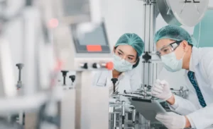
The exacting demands of semiconductor fabrication leave virtually no margin for error, where the integrity of sensitive electronics during production can be compromised by seemingly minor environmental factors such as temperature fluctuations, humidity levels, and airborne particulates. Understanding these pervasive challenges and the sophisticated, multi-layered methods deployed to counteract them is fundamental not only for producing reliable semiconductors but also for ensuring the robust performance of the enclosures designed to protect them in their operational lives. This relentless pursuit of environmental mastery underpins the functionality and longevity of nearly every electronic device in the modern world.
The Unseen Threat: Particulate Contamination and the Rise of Cleanrooms
At the microscopic level, airborne dust and chemical contaminants pose a relentless threat to the semiconductor manufacturing process. A single particle, often invisible to the naked eye and measuring just a few micrometers (a fraction of the diameter of a human hair), can settle on a silicon wafer. Such a minuscule intrusion can lead to catastrophic defects, ranging from short circuits in densely packed circuitry to interference with the delicate photolithography process, effectively rendering an entire chip unusable. Given that modern semiconductor features are often measured in single-digit nanometers, these contamination risks make particle control the most critical and foundational aspect of electronics manufacturing.
To combat this pervasive challenge, fabrication facilities operate within strictly controlled environments known as cleanrooms. These specialized spaces are engineered to maintain exceptionally low levels of airborne particles through a combination of advanced filtration systems, meticulously managed airflow, and stringent operational protocols. Cleanrooms are classified according to the ISO 14644-1 standard, which dictates the maximum number of particles permitted per cubic meter of air at specified particle sizes. For instance, an ISO Class 5 cleanroom, commonly used for critical semiconductor steps, allows no more than 3,520 particles of 0.5 micrometers or larger per cubic meter. In stark contrast, an ISO Class 7 facility, suitable for less sensitive assembly, permits up to 352,000 particles at the same size threshold. The most stringent cleanrooms, such as ISO Class 1, limit particles to just 10 per cubic meter at 0.1 micrometers, showcasing the extraordinary levels of cleanliness required for cutting-edge chip production.
Within these controlled environments, sophisticated air handling systems continuously circulate air through high-efficiency particulate air (HEPA) and ultra-low particulate air (ULPA) filters, which can capture particles as small as 0.1 micrometers with efficiencies exceeding 99.999%. This filtered air is often delivered in a laminar (unidirectional) flow pattern, sweeping particles away from critical work surfaces. Furthermore, cleanrooms typically maintain a positive pressure relative to adjacent areas. This design ensures that when doors are opened, air flows out of the cleanroom, preventing unfiltered outside contaminants from entering.
Personnel working in cleanrooms are another potential source of contamination. To mitigate particle shedding from skin and clothing, they must adhere to rigorous protocols, including wearing specialized garments known as "bunny suits," which cover the entire body. Before entering production areas, individuals pass through air showers that blast them with filtered air to dislodge any remaining surface particles. Regular cleaning and maintenance schedules for equipment, surfaces, and infrastructure are also paramount, preventing contamination buildup that could compromise sensitive processes and yield rates. The economic implications of contamination are immense; a single batch of wafers, if contaminated, can represent millions of dollars in lost revenue, underscoring the vital role of these elaborate control measures.
The Dual Challenge: Humidity, Static, and Their Impact on Fabrication
Beyond particulates, the precise control of atmospheric moisture presents a complex, two-sided challenge for semiconductor and enclosure manufacturers. Relative humidity (RH) must be carefully balanced to prevent both electrostatic discharge (ESD) events and material degradation.
When relative humidity drops below approximately 30-40%, the air becomes an effective insulator, allowing static electrical charge to build up more readily on surfaces, equipment, and even personnel. The human body, for example, can generate thousands of volts of static electricity through simple movements like walking across a floor. A sudden discharge occurs when a technician or tool makes contact with sensitive components. These electrostatic discharge events, lasting mere nanoseconds, can transfer thousands of volts of electricity instantly, irreversibly degrading or destroying nanoscale circuits. Such damage can be catastrophic, rendering a chip useless, or insidious, causing latent defects that lead to premature product failure in the field—a scenario far more costly due to warranty claims and reputational damage. The problem is exacerbated by the ever-shrinking geometries of modern chips, where smaller features are more susceptible to lower energy ESD events.
Conversely, excessive humidity creates different but equally serious problems. When moisture levels rise above 60%, water vapor can penetrate protective layers on metal components, initiating electrochemical reactions that lead to corrosion. Materials used in the fabrication process, particularly those in wet chemical baths or etching steps, can degrade under sustained exposure to high humidity. A critical process, photolithography, also becomes vulnerable; high humidity interferes with the adhesion of photoresist—light-sensitive materials applied in thin layers to wafer surfaces. Water molecules can prevent proper bonding between the photoresist and the silicon substrate, leading to patterns that are blurred, distorted, or completely lifted, resulting in defective chips. Furthermore, high moisture content can contaminate chemical processes, promoting unwanted reactions that alter material properties or introduce impurities.
To navigate this narrow operational window, manufacturing facilities typically maintain humidity levels between 40% and 60% RH. This range is considered optimal for dissipating static charges without promoting corrosion or compromising critical chemical processes. Sophisticated environmental control systems continuously monitor and adjust humidity levels throughout production areas using an array of sensors and feedback loops. Dehumidification equipment, such as desiccant dehumidifiers or refrigerated coils, removes excess water vapor during humid weather, while humidifiers add atmospheric content when conditions become too dry. Some advanced facilities employ separate humidity zones for different process steps, recognizing that certain stages may have slightly different optimal moisture requirements. The meticulous management of humidity is thus a critical ballet between preventing static destruction and averting moisture-induced degradation, all within an environment measured by nanometers.
The Precision Imperative: Temperature Stability in Fabrication
In the realm of semiconductor fabrication, where features are measured in nanometers and layers must align with sub-micron precision, even minor thermal fluctuations can create significant alignment challenges. Silicon wafers, along with the photolithography masks used to project circuit patterns, exhibit thermal expansion and contraction. While these dimensional changes occur on an extremely small scale, they become highly problematic when working with the atomic-level accuracy required for modern chip manufacturing.
The coefficient of thermal expansion (CTE) of silicon is relatively low, but over the surface of a 300mm wafer, a temperature variation of just a few tenths of a degree Celsius can cause sub-micron shifts. During photolithography, this expansion or contraction can lead to misalignment errors between successive layers of circuitry. Imagine trying to precisely overlay a pattern onto another pattern, where both are subtly growing or shrinking. Even slight variations of a fraction of a degree Celsius can shift the positions of features enough to cause devastating misalignment, resulting in non-functional devices. The optics within the photolithography tools themselves, comprising numerous lenses and mirrors, are also susceptible to thermal expansion, further complicating the challenge.
Modern semiconductor fabrication facilities maintain temperature control within an astonishing fraction of a degree Celsius—often ±0.1°C or even tighter—throughout their production areas. This level of stability is achieved through meticulously designed heating, ventilation, and air conditioning (HVAC) systems. Carefully engineered ductwork and diffusers distribute conditioned air evenly, eliminating hot or cold spots that could introduce localized thermal variations. The building construction itself often incorporates significant thermal mass, buffering against external temperature swings and creating a stable internal envelope.
Beyond ambient room temperature control, dedicated cooling systems are integrated directly with heat-generating equipment, such as plasma etchers, ion implanters, and lithography steppers, to prevent localized temperature rises from affecting nearby processes or the tool itself. These systems often employ recirculating chillers and liquid cooling lines to extract heat efficiently. Some of the most advanced facilities go a step further, isolating the most temperature-sensitive equipment within specialized micro-environments or chambers. In these contained spaces, conditions can be maintained with even greater precision, ensuring consistency regardless of minor fluctuations in the surrounding cleanroom environment. This multi-tiered approach to temperature management is indispensable for achieving the nanometer-scale accuracy that defines contemporary semiconductor manufacturing.
Engineering Resilience: Advanced Fabrication Methods and Materials

The ongoing battle against environmental variables has spurred significant innovation in both semiconductor and sensor enclosure manufacturing techniques, leading to methods that build inherent resilience into the products and processes. This involves not only controlling the environment but also designing tools and materials that can compensate for any residual variability.
In enclosure fabrication, maintaining laser-cutting accuracy despite fluctuating temperatures and humidity is crucial. Laser cutting systems, for example, must account for thermal expansion in both the cutting apparatus and the materials being processed. Manufacturers frequently calibrate their tools and implement real-time monitoring systems that detect and compensate for environmental drift. Modern laser systems employ embedded sensors that continuously measure beam characteristics, allowing for automatic adjustments when changes in temperature or humidity begin to affect performance, ensuring consistent cut dimensions.
Material science plays a critical role in providing another layer of environmental resilience. Alloys and composite materials are selected based on their dimensional stability across wide temperature ranges (low coefficients of thermal expansion). For sensor enclosures, surface treatments and specialized coatings create robust barriers that block water intrusion, preventing corrosion and protecting internal components from environmental exposure. These protective layers ensure structural integrity and long-term reliability in diverse operating conditions.
Within semiconductor fabrication, similar precision controls are embedded throughout the wafer processing sequence. Specialized equipment often creates isolated micro-environments or process chambers that shield critical steps—such as atomic layer deposition (ALD) or extreme ultraviolet (EUV) lithography—from external temperature and humidity variations. This containment strategy ensures that, even if ambient conditions in the cleanroom fluctuate slightly, the immediate processing environment remains impeccably stable.
Optical systems used in photolithography tools include highly advanced active alignment features. These systems utilize interferometers and feedback loops to continuously monitor the position of the wafer and the mask relative to the optical column. As components subtly heat up or cool down during operation, these systems automatically adjust their positioning and focus in real time, compensating for thermal drift to maintain nanometer-scale accuracy. This dynamic compensation is vital for achieving the multi-layer alignment required for advanced chip architectures.
Furthermore, sophisticated metrology tools are integrated at various stages to continuously verify that each process step produces results within acceptable tolerances. These automated measurement systems can detect even minor environmental shifts or process deviations before they cause defects, triggering immediate corrections or alerts. This "smart manufacturing" approach allows production to continue with minimal interruption, as environmental shifts are detected and corrected preemptively.
A Broader Lens: Industry-Wide Environmental Stewardship
The sheer scale of semiconductor manufacturing creates environmental challenges that extend far beyond what individual facilities can address through internal controls alone. The industry’s massive production volumes consume prodigious amounts of energy and water, while the highly specialized processing chemicals required for fabrication necessitate strict handling protocols and complex, specialized disposal methods. These realities have driven manufacturers, regulators, and industry organizations to forge collaborative partnerships aimed at developing sustainable practices that meet escalating production demands while simultaneously reducing environmental impact.
The semiconductor industry’s engagement with government agencies, such as the U.S. Environmental Protection Agency (EPA), focuses on reducing its environmental footprint while maintaining stringent production standards. These programs often address emissions reduction, water conservation, and chemical management through voluntary commitments that frequently exceed minimum regulatory requirements. Facilities actively participate in industry-wide initiatives, sharing best practices, technological advancements, and research findings. This collaborative approach allows smaller manufacturers to adopt proven sustainability technologies and methodologies without duplicating significant research and development costs, fostering widespread improvement across the sector.
Energy efficiency upgrades form a cornerstone of many sustainability efforts. Newer generations of manufacturing tools are designed to consume less electricity while maintaining or even increasing production output. Innovations in building management systems, smart lighting, and optimized HVAC systems also contribute to substantial energy savings. The industry is increasingly investing in renewable energy sources, such as solar and wind power, to power its fabrication plants, aiming for ambitious "net-zero" carbon emission targets.
Water conservation is another critical area. Semiconductor manufacturing requires vast quantities of ultrapure water for cleaning wafers and various chemical processes. To mitigate this demand, facilities are implementing advanced water recycling systems. These closed-loop systems treat and reuse process water, often circulating the same water through multiple purification cycles, dramatically reducing the reliance on fresh water supplies. This approach is particularly valuable in regions facing water scarcity, where industrial growth might otherwise be limited.
Chemical management programs focus on two key strategies: first, substituting safer, greener alternatives wherever possible without compromising product quality or performance; and second, refining processes to generate less hazardous waste from the outset. This involves optimizing chemical recipes, improving process efficiency, and investing in advanced waste treatment technologies to neutralize or recover valuable materials.
The semiconductor industry increasingly recognizes that robust environmental stewardship is not merely a regulatory burden but a fundamental component of long-term viability and competitive advantage. Sustainable operations ensure continued access to vital resources, streamline regulatory approvals, and enhance brand reputation. This commitment enables manufacturers to meet the ever-growing global demand for electronic devices across consumer, industrial, and automotive markets, while simultaneously demonstrating corporate responsibility.
The Future of Resilient Electronics: Ever-Increasing Demands
As electronics continue their relentless march towards greater complexity with each successive generation of technology, the demands placed on environmental controls in semiconductor fabrication and enclosure manufacturing will only intensify. The pursuit of smaller feature sizes (now entering the angstrom scale), tighter tolerances, and the integration of novel materials (such as 2D materials or those for quantum computing) will necessitate even more sophisticated and granular environmental management.
The future will likely see the widespread adoption of artificial intelligence and machine learning algorithms to predict and proactively adjust environmental conditions, moving beyond reactive control systems. "Smart cleanrooms" equipped with dense networks of sensors will provide real-time data on every conceivable environmental parameter, allowing for dynamic optimization and predictive maintenance. Advanced material science will continue to yield components with even greater inherent resilience to thermal and chemical stress.
The industry’s capacity to innovate in environmental control will directly correlate with its ability to continue pushing the boundaries of technological advancement. As electronic devices become more pervasive and integrated into every facet of human life, the foundational reliability provided by meticulously controlled manufacturing environments will remain paramount. The field will advance not only through breakthroughs in chip design but also through continuous development of better methods for managing the subtle, yet profoundly impactful, conditions that govern quality and reliability at the atomic scale.