In a landmark achievement for the field of quantum photonics, researchers at the University of Technology Sydney (UTS) have demonstrated a groundbreaking method for controlling quantum light sources by manipulating atomically thin layers of hexagonal boron nitride (hBN). By physically twisting these layers, the team has successfully managed to tune the properties of quantum emitters, marking a significant step toward the practical implementation of quantum computing, secure communication networks, and next-generation sensing technologies. This discovery addresses one of the most persistent challenges in quantum physics: the ability to reliably and precisely control the behavior of microscopic light sources within solid-state materials.
The study, led by Dr. Angus Gale and supervised by Professor Igor Aharonovich, focuses on the unique properties of hexagonal boron nitride, a two-dimensional material often referred to as "white graphene." Unlike traditional three-dimensional semiconductors, hBN’s layered structure allows for a level of mechanical manipulation previously thought impossible. The UTS team found that by rotating one layer of the material relative to another—a field of study known as "twistronics"—they could fundamentally alter the wavelength and color of the light emitted by defects within the crystal lattice. These defects, which act as quantum emitters or single-photon sources, are the fundamental building blocks for many proposed quantum hardware architectures.
The Evolution of Quantum Emitters and the Challenge of Control
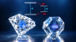
To understand the significance of the UTS breakthrough, it is necessary to examine the broader context of quantum light sources. Quantum emitters are systems that can release a single photon at a time. This capability is essential for quantum key distribution (QKD), which allows for unhackable communication, and for quantum computers, which use photons to carry information between processors. For decades, researchers have looked toward solid-state hosts like diamond and silicon carbide to house these emitters. While these materials are effective, they are also rigid. Once a quantum emitter is embedded within a diamond crystal, its properties are largely fixed. Tuning the emitter to a specific frequency—essential for ensuring different components of a quantum network can "talk" to one another—requires complex external setups involving extreme pressure, temperature shifts, or high-voltage electric fields.
The transition to two-dimensional materials like hexagonal boron nitride has changed the paradigm. Hexagonal boron nitride is composed of nitrogen and boron atoms arranged in a honeycomb lattice, similar to graphene. Because these layers are held together by weak van der Waals forces, they can be exfoliated into sheets that are only one atom thick. In 2015, it was discovered that hBN hosts bright, stable quantum emitters that can operate at room temperature, a massive advantage over other materials that require cryogenic cooling. However, even with hBN, the problem of precise, scalable tuning remained. The UTS team’s approach of using mechanical "twisting" provides a direct, physical lever to solve this problem.
Methodology: The Mechanics of Twisting Nanomaterials
The experimental process conducted by Dr. Gale and his colleagues involved a sophisticated "pick-and-place" technique. Unlike conventional semiconductor manufacturing, where materials are grown in fixed layers, the researchers utilized the layered nature of hBN to create a dynamic system. They were able to isolate a single layer of hBN, place it atop another, and then use specialized equipment to rotate the top layer to a precise angle.
"We’re leveraging the fact that this material, hexagonal boron nitride, is layered," Dr. Gale explained. "We can pick it up, stack it, twist it, and use that twist to modify the emitters. You can’t really do that with traditional materials like diamond or silicon carbide."
The team discovered that the magnitude of the change in light emission was far greater than what is typically achieved through other tuning methods. By changing the twist angle, they could shift the emission wavelength by a significant margin. This phenomenon is attributed to the creation of moiré patterns—interference patterns that emerge when two similar templates are overlaid at an offset. These patterns create a new periodic potential energy landscape that the quantum emitters reside in, effectively changing the electronic environment around the defect and thus altering the light it produces.
One of the most notable aspects of the UTS experiment was its repeatability. Most studies in the field of twistronics involve creating a device at a specific angle and measuring it. The UTS researchers, however, demonstrated that they could repeatedly lift, rotate, and restack the material. This proves that the tuning is not a one-time fluke of fabrication but a controllable, reversible physical process.
Technical Data and Observations
The data gathered during the experiments revealed that the spectral shifts observed were "much larger than expected." In traditional solid-state systems, tuning the wavelength of an emitter often involves "strain engineering," where the material is physically stretched. However, the amount of strain a crystal can withstand before breaking is limited, usually resulting in a tuning range of only a few nanometers.
The twisting method employed by the UTS team allows for a much broader range of manipulation. By altering the atomic alignment, the researchers influenced the local strain and the electronic coupling between the layers. This resulted in a dramatic shift in the energy levels of the quantum defects. The researchers noted that rather than trying to force hBN to behave like a rigid 3D crystal, they embraced its "weakness"—its layered, flexible nature—and turned it into a strength.
This ability to shift emission by a significant amount is critical for the "interference" of photons. For two photons to be used in a quantum logic gate, they must be identical in wavelength and wave-shape. Because no two quantum emitters are naturally identical due to microscopic variations in their environment, a "tuning lever" is required to bring them into alignment. The UTS discovery provides exactly that.
A New Analogy for Quantum Materials
To illustrate the difference between hBN and traditional materials, Dr. Gale used a culinary analogy. He compared materials like diamond to a solid block of cheese and hBN to a stack of sliced cheese.
"With a block of cheese, you can’t really get to the flavor in the middle. But with slices, you can peel away layers, put them back together and change how they interact," Gale said. This accessibility is what allows researchers to manipulate the interior environment of the material at the atomic level. By reaching into the "middle" of the stack and rotating a slice, they can change the "flavor"—or in this case, the light frequency—of the entire system.
Implications for Future Technology
The potential applications for this technology span several high-priority sectors, including cybersecurity, healthcare, and navigation. Professor Igor Aharonovich, the supervising author of the study, emphasized that the ability to twist materials reveals entirely new physical behaviors that were previously inaccessible.
"You can take two layers that don’t do much on their own, put them together at a specific angle, and suddenly you have a completely different system," Professor Aharonovich said. He believes these findings are a catalyst for several emerging fields:
- Quantum Computing: In the race to build a scalable quantum computer, photons are the preferred choice for transmitting data between qubits. The ability to tune emitters ensures that different parts of a quantum computer can operate in harmony, reducing error rates and increasing processing power.
- Cybersecurity: Quantum Key Distribution (QKD) relies on the laws of physics to secure data. By using single photons to create encryption keys, any attempt to intercept the data would change the state of the photons, instantly alerting the users. Twistable hBN emitters could lead to more compact and efficient QKD devices for secure government and financial communications.
- Healthcare and Sensing: Quantum sensors are capable of detecting infinitesimal changes in magnetic and electric fields. Professor Aharonovich noted that these could be used to improve MRI technology, allowing for molecular-level imaging within the human body, or to develop ultra-sensitive diagnostic tools for early disease detection.
- Navigation and GPS: In environments where GPS signals are blocked or jammed, quantum sensors can provide "inertial navigation" with extreme precision. The control offered by the UTS method could help miniaturize these sensors for use in autonomous vehicles or aerospace technology.
Chronology of the Research and Global Context
The research at UTS did not happen in a vacuum. It is part of a global surge in interest regarding 2D materials and quantum photonics.
- 2004: The discovery of graphene at the University of Manchester kicks off the 2D materials revolution.
- 2010s: Researchers identify hexagonal boron nitride as an excellent insulator and a potential host for quantum emitters.
- 2015-2016: Significant papers (including several from UTS) confirm that hBN can host single-photon emitters that work at room temperature.
- 2018: The "Magic Angle" discovery in graphene (showing that a 1.1-degree twist creates superconductivity) ignites the field of twistronics.
- 2023-2024: The UTS team successfully applies the principles of twistronics to quantum light sources, moving beyond electronic properties to optical properties.
This timeline shows a rapid progression from fundamental material science to functional quantum engineering. The UTS team’s work represents the convergence of 2D material science and quantum optics, two fields that were previously operating in parallel.
Analysis of the Path Forward
While the UTS demonstration is a major milestone, the path to commercialization involves several more steps. The current experiments were conducted in a controlled laboratory setting using specialized microscopy and nanomanipulation tools. To bring this to the mass market, the "twist-and-stack" process would need to be automated at scale.
However, the industry reaction to this line of research has been overwhelmingly positive. Tech giants like IBM, Google, and Amazon, who are heavily invested in quantum hardware, are increasingly looking at solid-state platforms that can operate outside of massive, expensive dilution refrigerators. A material like hBN, which can be tuned mechanically and operates at room temperature, offers a compelling alternative to the superconducting qubits currently favored by some firms.
Furthermore, the "twistable" platform opens up a new playground for theoretical physicists. The interaction between the layers and the resulting moiré potential is complex, and the UTS study provides a wealth of data for theorists to refine their models of how light and matter interact at the nanoscale.
Conclusion
The work of Dr. Angus Gale, Professor Igor Aharonovich, and their team at the University of Technology Sydney has provided the scientific community with a powerful new "lever" for quantum technology. By showing that the simple act of twisting an atomically thin material can yield unprecedented control over quantum light, they have moved the field one step closer to a future where quantum devices are as common and practical as the silicon chips of today. As the researchers continue to refine this technique, the focus will shift toward integrating these twistable emitters into complex integrated circuits, paving the way for the next generation of the information age.