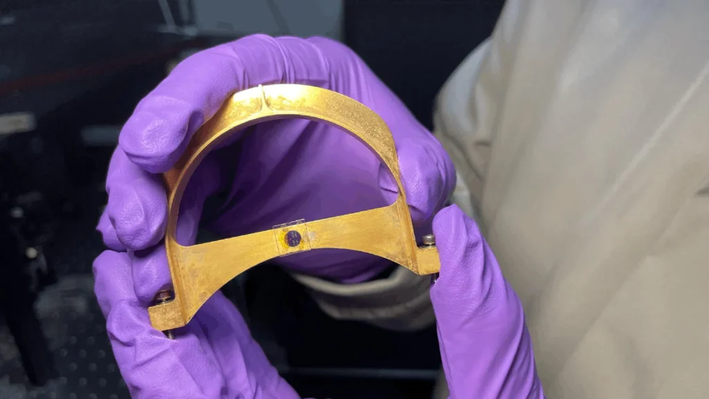
Quantum computers, long hailed as the next frontier in computation and communication, currently face formidable obstacles rooted in their fundamental operational requirements. Predominantly, these nascent machines necessitate environments cooled to temperatures approaching absolute zero – a frigid -459 degrees Fahrenheit (or roughly a few millikelvin) – to sustain the exquisitely fragile quantum states essential for their function. This extreme cryogenic demand translates into immensely complex, voluminous, and exorbitantly expensive infrastructure, severely limiting their accessibility and widespread deployment. However, a recent breakthrough from Stanford University promises to redefine this paradigm, as researchers have successfully engineered a nanoscale optical device capable of operating at room temperature while robustly linking the quantum properties of light and electrons. This pivotal advancement could significantly accelerate the development of smaller, lower-cost quantum technologies, crucially enabling the secure and efficient transmission of quantum information over long distances.
The newly developed device represents a critical step towards practical quantum communication systems by facilitating entanglement between photons, the elementary particles of light, and electrons. This intricate quantum connection is universally recognized as a foundational requirement for building future quantum networks and distributed quantum computing architectures. Jennifer Dionne, a professor of materials science and engineering at Stanford and the senior author of the groundbreaking study published in Nature Communications, emphasizes the innovative application of existing materials. "The material in question is not really new, but the way we use it is," Dionne states. "It provides a very versatile, stable spin connection between electrons and photons that is the theoretical basis of quantum communication. Typically, however, the electrons lose their spin too quickly to be useful, making this stability a key differentiator."
Overcoming the Cryogenic Barrier: A Historical Challenge
The pursuit of quantum computing has been intrinsically linked with the challenge of extreme cold since its inception. Early theoretical work in the 1980s by pioneers like Richard Feynman posited the potential of quantum systems to simulate physical phenomena beyond the reach of classical computers. Yet, realizing these theoretical constructs in practice proved immensely difficult. Quantum states, such as superposition and entanglement, are extraordinarily delicate and prone to a phenomenon called decoherence, where interactions with the environment cause them to lose their quantum properties and revert to classical states.
For decades, the primary strategy to combat decoherence has been to isolate quantum systems as much as possible, with cryogenic cooling being the most effective method for many leading qubit modalities. Superconducting qubits, for instance, which are at the heart of many prominent quantum computing efforts by companies like IBM and Google, require dilution refrigerators capable of reaching temperatures colder than deep space, typically in the millikelvin range (thousandths of a degree above absolute zero). These refrigerators are massive, consume significant power, and are incredibly costly, often exceeding several million dollars per unit. Trapped ion qubits, another promising modality, operate at slightly higher temperatures but still demand ultra-high vacuum environments and precise laser cooling. The logistical and financial overhead associated with these requirements has been a major bottleneck, confining quantum computing to specialized laboratories and hindering its transition to broader commercial or industrial applications. The Stanford team’s innovation directly confronts this fundamental barrier by demonstrating a functional quantum device at ambient temperatures, offering a compelling alternative path forward.
The Ingenious Design: Twisted Light and Quantum Spin
At the heart of Stanford’s breakthrough is a meticulously engineered device that synergistically combines a thin, patterned layer of molybdenum diselenide (MoSe2) with a nanopatterned silicon substrate. Molybdenum diselenide belongs to an exciting class of materials known as transition metal dichalcogenides (TMDCs), which have garnered significant attention in materials science for their extraordinary optical, electronic, and quantum properties. These materials often exhibit strong spin-orbit coupling, meaning the spin of an electron is intimately linked to its motion, a property crucial for manipulating quantum states.
The silicon nanostructures within the device play an indispensable role by generating what the researchers term "twisted light." Feng Pan, a postdoctoral scholar in Dionne’s lab and the first author of the Nature Communications paper, elaborates on this fascinating phenomenon: "The silicon nanostructures enable what we call ‘twisted light.’ The photons spin in a corkscrew fashion, but more importantly, we can use these spinning photons to impart spin on electrons that are the heart of quantum computing." This "twisted light" refers to photons carrying orbital angular momentum (OAM), a property distinct from their polarization (spin angular momentum). While conventional light sources emit photons with well-defined polarization, twisted light introduces a helical wavefront, effectively spinning around its axis of propagation. This OAM can be precisely controlled and transferred, making it an excellent candidate for encoding quantum information and for interacting with the spin of electrons.
Dionne underscores the astonishing scale of this engineering feat: "The patterned nanostructures are imperceptible to the human eye, about the size of the wavelength of visible light." These structures, despite their minuscule dimensions (nanometers), allow for the exquisite manipulation of photons. "They help us manipulate photons very precisely to make them spin – to twist them – in a specific direction, for example, up or down," she adds. This precise control over the OAM of photons, coupled with the unique properties of MoSe2, is what enables the stable, room-temperature entanglement.
A Simpler Path to Quantum Communication and Beyond
The ability to use twisted light to entangle with electron spins is fundamental to creating qubits, the basic building blocks of quantum information systems. Unlike classical bits, which can only exist in a state of 0 or 1, qubits leverage quantum mechanical effects such as superposition (being both 0 and 1 simultaneously) and entanglement (being intrinsically linked, even when separated) to process and transmit information in entirely novel and powerful ways. The stability of these quantum states is paramount, and decoherence remains the single largest hurdle in scaling quantum technologies.
By operating at room temperature, the Stanford device circumvents one of the most formidable obstacles that has historically limited the widespread adoption and practical utility of quantum technologies. The inherent complexity and cost of cryogenic cooling systems have restricted quantum research and development to a select few, well-funded institutions. The compact and relatively inexpensive design of this new device, compared to the sprawling infrastructure of current cryogenic quantum systems, opens doors to a much broader range of applications and users. This accessibility could democratize quantum research, allowing more innovators to contribute to the field and accelerate progress.
The implications for quantum communication are particularly profound. Secure communication is a global imperative, and quantum key distribution (QKD) offers theoretically unbreakable encryption by leveraging the principles of quantum mechanics. Existing QKD systems often rely on photonic qubits, but integrating them with stable, room-temperature electron spins could enable more robust and versatile quantum repeaters, essential for extending quantum communication over continental distances. If further developed, this technology could contribute significantly to advances in secure communications, laying the groundwork for a truly quantum internet. Beyond communication, the potential extends to advanced sensing, where quantum sensors can achieve unprecedented precision; high-performance computing, enabling solutions to problems intractable for classical supercomputers; artificial intelligence, by powering novel quantum algorithms; and other emerging applications such as drug discovery and materials science, by simulating molecular interactions at a quantum level.
Why the Material Matters: The Role of TMDCs
The selection of molybdenum diselenide (MoSe2) as the active quantum material was not arbitrary. The research team specifically chose TMDC materials due to their extraordinary quantum characteristics. This strategic choice was bolstered by collaboration with Stanford researchers Fang Liu and Tony Heinz, who are leading experts in these advanced materials. TMDCs, a class of two-dimensional (2D) materials similar to graphene, possess unique properties that make them highly attractive for optoelectronic and quantum applications. They exhibit a direct bandgap in their monolayer form, meaning they efficiently absorb and emit light. Crucially, they also possess strong exciton physics (bound electron-hole pairs) and spin-valley coupling, where the spin of an electron is linked to its momentum valley in the material’s electronic band structure. These properties enable efficient conversion between photons and electrons while preserving quantum information.
"It all comes down to this material and our silicon chip," Pan reiterates, emphasizing the synergy. "Together, they efficiently confine and enhance the twisting of light to create a strong coupling of spin between photons and electrons. This stabilizes the quantum state that makes quantum communication possible." The robust interaction between light and matter is paramount for quantum operations. In conventional materials, this interaction is often weak, leading to rapid decoherence. However, the specific combination of MoSe2 with the nanopatterned silicon allows for an amplified and precisely controlled interaction, helping to preserve the delicate quantum properties necessary for communication and computing tasks at temperatures that are far more practical than previously imagined. The device’s ability to stabilize the electron spin, which is notoriously fragile, at room temperature is a testament to the effectiveness of this material-structure combination.
Toward Future Quantum Networks and Everyday Integration
The Stanford team is not resting on its laurels. The researchers are actively engaged in refining the current device, exploring an array of additional TMDC materials and innovative material combinations that could yield even greater performance and efficiency. They are also investigating whether these novel room-temperature systems might unveil entirely new quantum capabilities or phenomena that are currently inaccessible or unobservable at standard operating temperatures. This ongoing exploration is crucial for pushing the boundaries of what is possible in quantum science.
A more ambitious, longer-term objective involves seamlessly integrating devices of this nature into larger, more complex quantum networks. Achieving this grand vision will necessitate significant advancements and improvements in a host of supporting technologies. These include more efficient and stable light sources, high-speed quantum modulators for encoding information, highly sensitive quantum detectors, and robust interconnects capable of transmitting quantum information without degradation. The development of scalable quantum repeaters, which can extend entanglement over long distances by periodically "refreshing" quantum signals, is particularly vital for building a global quantum internet.
Ultimately, the aspiration is to miniaturize quantum components to such an extent that they can be seamlessly incorporated into everyday electronics, transforming our interaction with technology. While such a future remains many years, perhaps even decades, away, the work undertaken by the Stanford team represents a monumental stride toward making quantum technology not only more accessible but also significantly more practical. "If we can do that, maybe someday we could do quantum computing in a cell phone," Pan envisions with a smile, acknowledging the ambitious scope of this future. "But that’s a 10-plus-year plan." This long-term perspective highlights the phased approach required for such transformative technology, moving from fundamental research to integrated systems and eventually to widespread consumer applications. The success of this research provides a tangible roadmap and renewed optimism for a quantum future that is not confined to specialized laboratories but accessible to all. The economic implications are vast, as reducing the barrier to entry for quantum technologies could unlock new industries, foster innovation, and enhance national security through impenetrable communication channels.