The global pursuit of ultra-efficient electronics has reached a significant milestone as researchers at Chalmers University of Technology in Sweden have unveiled a pioneering method to stabilize superconductivity under conditions that typically cause the phenomenon to collapse. By shifting the focus from the chemical composition of superconducting materials to the physical architecture of the surfaces upon which they are grown, the team has successfully demonstrated that "sculpting" a substrate at the nanoscale can induce superconductivity at higher temperatures and maintain it within intense magnetic fields. This development, published in the journal Nature Communications, addresses two of the most persistent technical hurdles in the field of condensed matter physics and offers a potential roadmap for the integration of superconductors into mainstream digital infrastructure, quantum computing, and energy sectors.
The Growing Crisis of Global Energy Consumption in ICT
The urgency behind this research is driven by the staggering energy requirements of the modern digital age. Current estimates suggest that information and communications technology (ICT) networks, data centers, and personal digital devices are responsible for between 6 and 12 percent of total global electricity consumption. As artificial intelligence, cloud computing, and the Internet of Things (IoT) continue to expand, this figure is projected to rise sharply. Traditional silicon-based electronics operate through the movement of electrons through resistive materials, a process that inherently generates heat. This "Joule heating" represents a massive waste of energy, requiring additional power for cooling systems in massive server farms.
Superconductors offer a theoretical solution to this inefficiency. These materials possess the unique ability to conduct electricity with zero resistance, meaning no energy is lost as heat during transmission. If superconductors could be integrated into standard electronic components, power grids, and data processing units, the efficiency of these systems could increase by orders of magnitude. However, the transition from laboratory curiosity to industrial application has been stalled for decades by the extreme environmental requirements of known superconducting materials.
Understanding the Barriers: Temperature and Magnetic Interference
Superconductivity is a quantum mechanical state where electrons form "Cooper pairs" that move through a lattice without scattering. Historically, this state was only achievable at temperatures near absolute zero (0 Kelvin or -273.15 degrees Celsius). While the discovery of high-temperature superconductors (HTS) in the 1980s—specifically the cuprate family—raised the operating threshold to around 77 Kelvin (-196 degrees Celsius), this still necessitates the use of liquid nitrogen or complex cryocoolers.
Beyond the temperature constraint, magnetic fields pose a second, equally daunting challenge. In many superconductors, a strong magnetic field can penetrate the material and disrupt the delicate alignment of electron pairs, effectively "killing" the superconducting state. This is a critical failure point for many envisioned applications. For example, quantum computers often require magnetic fields to manipulate qubits, and high-power electrical systems naturally generate electromagnetic fields. A superconductor that cannot withstand magnetic interference is of limited use in a modern technological environment.
A Paradigm Shift in Material Design
For years, the primary strategy for improving superconductors involved chemical doping—adding or substituting atoms within the material’s crystal lattice to alter its electronic properties. While this has yielded some successes, it is a process fraught with difficulty, particularly with cuprates, which have complex, brittle structures that are resistant to post-manufacturing modification.
The Chalmers team, led by Floriana Lombardi, Professor of Quantum Device Physics, opted for a structural rather than a chemical approach. Instead of trying to change the superconducting film itself, they focused on the substrate—the underlying material that serves as the foundation for the superconducting layer.
"By sculpting the surface that the superconductor rests on, we were able to induce superconductivity at significantly higher temperatures than previously possible," Professor Lombardi stated. "We also found that the material remained superconducting even when exposed to strong magnetic fields."
The Science of Nanofaceted Substrates
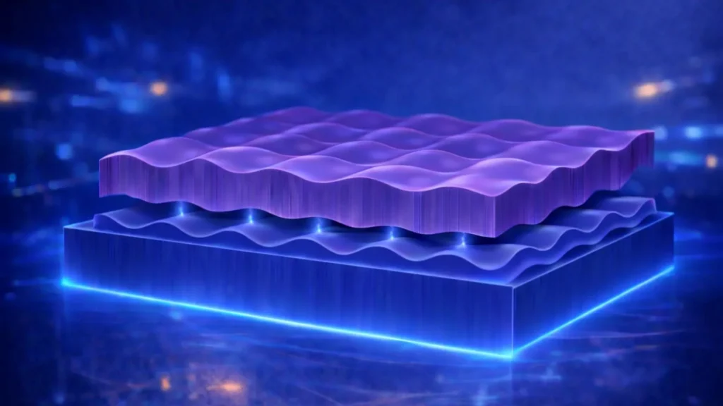
The researchers utilized an ultrathin film of Yttrium Barium Copper Oxide (YBCO), a well-known member of the cuprate family. The film used in the study was only a few nanometers thick—roughly one-thousandth the thickness of a strand of spider silk. At this scale, the interface between the superconducting film and the substrate becomes the dominant factor in determining the material’s behavior.
The breakthrough involved a two-step fabrication process. First, the substrate was treated in a high-temperature vacuum environment. This process triggered a self-organizing reaction on the surface, creating an orderly pattern of microscopic ridges and valleys, a process known as nanofaceting. When the YBCO atoms were deposited onto this "sculpted" surface, they did not settle in a flat, uniform layer. Instead, the atoms followed the template provided by the substrate’s ridges.
Eric Wahlberg, a researcher at RISE Research Institutes of Sweden and a key contributor to the study, explained that the specific arrangement of atoms in the substrate acts as a guide. "By changing the surface design of the substrate, we were able to influence the superconducting properties and ensure they were preserved," Wahlberg noted.
The resulting "nanofaceted" interface created a unique electronic environment. The researchers observed that the electrons in the YBCO film began to exhibit a "preferential direction" in their movement. This directional bias helped stabilize the Cooper pairs against thermal fluctuations and magnetic disruption, effectively "locking" the superconducting state in place under conditions that would normally destroy it.
Supporting Data and Experimental Results
The experimental data provided in the Nature Communications study highlights the robustness of this new approach. The team subjected the nanofaceted YBCO films to rigorous testing, including exposure to high-intensity magnetic fields. In traditional ultrathin cuprate films, superconductivity often begins to degrade at relatively low magnetic thresholds. However, the Chalmers-led team found that their engineered films maintained zero resistance even when subjected to significant magnetic flux.
Furthermore, the "critical temperature" (Tc)—the point at which a material transitions into a superconductor—was measurably higher in the films grown on sculpted substrates compared to those grown on standard flat surfaces. While the research does not yet achieve room-temperature superconductivity, the incremental increase in Tc and the dramatic increase in magnetic resilience represent a significant leap forward for thin-film superconductivity.
Chronology of the Discovery and International Collaboration
The development of this technique is the result of several years of interdisciplinary collaboration. The project brought together experts from several prestigious institutions across Europe and Asia, reflecting the global importance of the research.
- Initial Theory: The project began with theoretical modeling at Chalmers and Uppsala University, exploring how surface strain and interfacial geometry could influence electron pairing in cuprates.
- Substrate Fabrication: The high-temperature vacuum treatment was perfected at the Myfab Chalmers cleanroom facility, a state-of-the-art laboratory that allows for atomic-scale precision.
- Film Growth and Testing: The YBCO films were deposited using pulsed laser deposition. Subsequent testing was conducted at various facilities, including high-magnetic-field laboratories in France (Grenoble and Toulouse) to verify the material’s stability.
- Data Analysis: Researchers from Italy, India, and Germany contributed to the complex data analysis required to understand the electron behavior at the interface.
Funding for the project was provided by a coalition of major scientific bodies, including the Swedish Research Council (VR), the Knut and Alice Wallenberg Foundation, and the European Union’s EIC Pathfinder grant, which specifically targets high-risk, high-reward "deep tech" research.
Implications for Quantum Technology and Energy
The implications of this research extend far beyond the laboratory. In the field of quantum computing, one of the primary obstacles is "decoherence"—the loss of quantum information due to environmental noise, heat, or magnetic interference. Superconducting circuits are a leading candidate for building stable qubits, but they are notoriously sensitive. By using nanofaceted substrates, engineers may be able to create quantum components that are more robust and less prone to errors caused by external magnetic fields.
In the energy sector, the ability to maintain superconductivity in strong magnetic fields is a prerequisite for the development of compact fusion reactors and next-generation particle accelerators. High-field magnets are essential for confining plasma in fusion devices; if the superconducting tapes used in these magnets can be made more resilient through substrate engineering, it could lower the cost and complexity of clean fusion energy.
Additionally, the research offers a new design principle for the semiconductor industry. As the limits of Moore’s Law are reached, the industry is looking toward "More than Moore" technologies that incorporate new materials. Substrate engineering provides a way to enhance the performance of existing materials without the need for volatile chemical changes, making it a more viable path for industrial scaling.
Conclusion and Future Outlook
The work of the Chalmers University team represents a fundamental shift in how scientists approach the "superconductivity problem." By demonstrating that the physical topology of a substrate can be used as a tool to tune the quantum properties of a material, they have opened a new frontier in condensed matter physics.
"Instead of searching for entirely new materials or manipulating the chemical properties of existing ones, we are now showing how superconductivity can be enhanced by sculpting the substrate," Professor Lombardi concluded.
The next phase of research will likely involve testing this "sculpting" technique on other types of superconducting materials and exploring whether even more complex surface patterns could push the critical temperature closer to room temperature. If successful, the era of zero-loss electronics may be closer than previously imagined, potentially transforming the global energy landscape and the future of digital technology.