For decades, the analysis of materials’ chemical composition has been reliant on large, often prohibitively expensive laboratory instruments known as spectrometers. These sophisticated systems, fundamental to fields ranging from disease diagnosis and food quality control to environmental monitoring, traditionally operate by dispersing light into its constituent wavelengths using optical components like prisms or diffraction gratings. The inherent physics of this process necessitates a relatively long optical path for effective light separation, rendering these instruments inherently bulky and challenging to miniaturize for portable or integrated applications.
A Paradigm Shift in Spectral Analysis
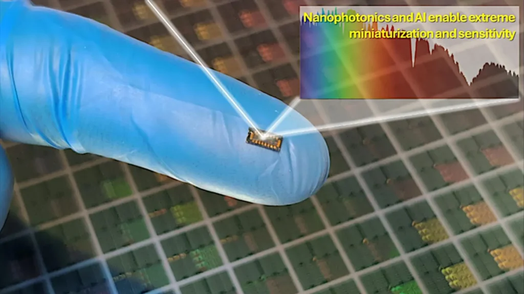
A groundbreaking development from researchers at the University of California Davis (UC Davis) now promises to fundamentally alter this landscape. As detailed in their recent publication in the prestigious journal Advanced Photonics, the team has successfully engineered a spectrometer-on-a-chip that dramatically redefines the scale and operational principles of spectral analysis. This novel device, astonishingly diminutive in size—approaching that of a single grain of sand—eschews conventional bulky optical components. Instead, it leverages the power of artificial intelligence (AI) in conjunction with an array of specially designed silicon sensors to computationally reconstruct the full light spectrum.
This innovation represents a significant leap forward, addressing a long-standing challenge in analytical instrumentation. The global market for spectrometers, valued at billions of dollars annually, underscores the critical importance of these devices. However, their traditional limitations in size, cost, and portability have often restricted their deployment to dedicated laboratory environments. The UC Davis breakthrough opens doors to a future where high-precision spectral analysis can be integrated into everyday devices, enhancing accessibility and enabling real-time insights across myriad applications.
Replacing Bulky Optics with Intelligent Computation
The core of this transformative technology lies in its departure from the standard optical method of physically spreading light into a rainbow of colors. The UC Davis chip employs a network of 16 distinct silicon detectors, each meticulously engineered to exhibit a unique and nuanced response to incident light. Rather than directly isolating individual colors, these detectors capture a complex array of encoded signals, each containing fragmented yet crucial spectral information.
To conceptualize this intricate process, one might consider the system analogous to a panel of highly specialized tasters, each sampling a different facet of a complex culinary mixture. Individually, no single taster perceives the complete flavor profile. However, when their collective, distinct sensory inputs are aggregated, they provide sufficient information for an expert palate—or in this case, a sophisticated AI algorithm—to accurately reconstruct the original, holistic flavor (or light spectrum).
The second, equally vital component of this system is a fully connected neural network. This AI architecture undergoes extensive training, learning from thousands of examples where known light spectra are correlated with the corresponding encoded signals generated by the chip’s detectors. Given that the raw detector signals are inherently noisy and highly encoded, the neural network is tasked with discerning the intricate, non-linear relationship between these seemingly disparate signals and the actual spectrum of light. This computational prowess enables the system to solve what researchers refer to as an "inverse problem"—deducing the original cause (the light spectrum) from its observed effects (the detector responses). The result is the ability to reproduce spectral data with remarkable accuracy, achieving a resolution of approximately 8 nanometers (nm) without the need for any bulky optical hardware. This computational approach not only facilitates miniaturization but also offers a level of flexibility and adaptability not easily achieved with fixed optical systems.
Expanding Spectral Horizons: Near-Infrared Detection
A pivotal engineering achievement embedded within this new architecture is the successful expansion of silicon’s spectral sensitivity, particularly into the near-infrared (NIR) range. Standard silicon photodiodes, while highly effective for detecting visible light, typically exhibit poor performance in capturing NIR light, which encompasses wavelengths up to 1100 nm. This limitation has historically been a significant hurdle, as NIR light is of paramount importance for a wide array of applications, particularly in biomedical imaging. NIR photons possess the unique ability to penetrate deeper into human tissues compared to visible light, making them invaluable for non-invasive diagnostics, such as monitoring blood oxygenation, detecting early-stage cancers, and even continuous glucose monitoring.
The UC Davis team overcame this inherent limitation by modifying the surface of standard silicon photodiodes with specialized photon-trapping surface textures (PTSTs). These intricately patterned surfaces fundamentally alter the behavior of light within the thin silicon layer. Instead of allowing NIR photons to pass directly through the material, the textured surface repeatedly scatters the incoming light. This repeated scattering significantly increases the optical path length within the silicon, thereby enhancing the likelihood that the silicon material will absorb the NIR photons. Consequently, this ingenious modification renders the chip sensitive across a much broader spectral range than conventional silicon sensors, bridging a critical gap in on-chip spectroscopy.
The development of PTSTs is a testament to advanced materials science and nano-fabrication techniques. By precisely controlling the interaction of light at the nanoscale, researchers have unlocked a previously inaccessible spectral window for compact silicon devices, paving the way for advanced biomedical sensors that can operate non-invasively and in real-time.
Capturing Ultrafast Light Interactions: Beyond Static Analysis
Beyond its unparalleled miniaturization and expanded spectral range, the new architecture introduces another revolutionary capability: the integration of high-speed sensors designed to measure photon lifetime with extraordinary temporal precision. This advanced feature allows the device to detect and analyze ultrafast interactions between light and matter—phenomena that traditional, slower spectrometers often miss entirely.
Ultrafast light-matter interactions occur on picosecond (10^-12 seconds) or even femtosecond (10^-15 seconds) timescales and are critical for understanding fundamental processes in chemistry, physics, and biology. For example, measuring fluorescence lifetime can provide detailed information about molecular environments, protein folding, and even the presence of specific biomarkers in biological samples. Traditional systems capable of such measurements are typically vast, complex, and extraordinarily expensive, often requiring dedicated laser facilities.
Researchers involved in the project emphasize that this ability to capture transient, ultrafast phenomena could unlock entirely new forms of sensing and imaging. Potential applications include advanced materials characterization, real-time monitoring of chemical reactions, and even novel approaches to medical diagnostics that probe the dynamic properties of biological tissues at a molecular level. The integration of such capabilities into a chip-scale device represents a monumental engineering feat, pushing the boundaries of what is possible in compact analytical instrumentation.
Tiny Footprint, Immense Potential: Engineering for Real-World Deployment
The culmination of these innovations is a complete spectrometer system that occupies an incredibly small footprint of just 0.4 square millimeters. Despite its minuscule size, the device maintains high sensitivity and exhibits robust resistance to electrical noise—a pervasive and often debilitating challenge for portable, low-cost electronic devices. The AI-assisted design plays a crucial role here, enabling the system to preserve clear signal quality even in electrically noisy environments, which are common in real-world applications outside of controlled laboratory settings.
This inherent robustness is critical for the widespread adoption and integration of the technology. The ability to perform reliable spectral analysis in challenging conditions makes the spectrometer-on-a-chip suitable for deployment in a diverse array of environments, from industrial manufacturing floors to remote agricultural fields and even within the human body.
The synergistic combination of advanced machine learning algorithms with enhanced silicon light detection capabilities is poised to pave the way for a new generation of compact, real-time hyperspectral sensing devices. The implications of this technology are far-reaching and transformative across multiple sectors:
Broader Impact and Implications
-
Healthcare and Biomedical Diagnostics: The most immediate and profound impact is anticipated in healthcare. The development of a portable, high-resolution spectrometer could revolutionize point-of-care diagnostics. Imagine wearable health monitors capable of continuous, non-invasive analysis of biomarkers for early disease detection, blood glucose levels, hydration status, or oxygen saturation. This could lead to personalized medicine on an unprecedented scale, allowing individuals and healthcare providers to monitor health proactively and make data-driven decisions in real-time. For instance, a device integrated into a smartwatch could potentially detect subtle changes in tissue composition indicative of disease long before symptoms manifest.
-
Food Safety and Quality Analysis: In the agricultural and food industries, this technology offers immense promise. Compact hyperspectral sensors could enable real-time analysis of produce quality, freshness, and ripeness directly in the field or at processing plants. They could also detect contaminants, pesticides, or adulterants in food products instantly, ensuring greater consumer safety and reducing waste. Farmers could optimize crop yields by monitoring plant health, nutrient deficiencies, or disease outbreaks with unprecedented precision.
-
Environmental Monitoring: The ability to deploy compact spectrometers in remote or challenging environments would significantly enhance environmental monitoring efforts. These devices could be integrated into drones, autonomous vehicles, or fixed sensor networks to monitor air and water quality, detect pollutants, identify hazardous materials, and track changes in atmospheric composition or ecosystem health. This real-time data collection could provide invaluable insights for climate science, pollution control, and disaster response.
-
Industrial Process Control and Material Science: In manufacturing and industrial settings, the spectrometer-on-a-chip could facilitate continuous, in-line quality control. Materials could be analyzed during production to ensure consistent composition, detect defects, or verify authenticity. This could lead to increased efficiency, reduced waste, and improved product reliability across various industries, from pharmaceuticals to advanced materials manufacturing.
-
Scientific Research and Education: Beyond commercial applications, this miniaturized technology will empower scientific research. Researchers could conduct experiments with spectral analysis in environments previously inaccessible, leading to new discoveries. Furthermore, the lower cost and portability could make advanced spectral analysis more accessible for educational purposes, inspiring the next generation of scientists and engineers.
Chronology and Future Outlook
The development of advanced spectrometers has followed a long trajectory, driven by the persistent demand for greater analytical precision and versatility. From the early prism-based instruments of the 17th century to the sophisticated grating-based systems of the 20th century, the core principle of light dispersion remained largely unchanged. The advent of silicon photonics in recent decades opened new avenues for integrating optical components onto chips, but the fundamental challenge of miniaturizing the necessary optical path remained.
The UC Davis team’s work, culminating in their publication in Advanced Photonics, represents a significant inflection point in this history. It marks a decisive shift towards computational spectroscopy, where the intelligence of AI compensates for physical limitations, allowing for unprecedented miniaturization without sacrificing performance. While the exact timeline for commercialization remains to be seen, this research lays a robust foundation. Further research will likely focus on optimizing the AI algorithms, refining the PTST designs for even broader spectral ranges, and exploring integration strategies with other sensor modalities.
Experts in the field of photonics and AI foresee a future where such chip-scale spectrometers become ubiquitous, much like cameras in smartphones today. "This development is not just an incremental improvement; it’s a paradigm shift," commented a leading photonics expert familiar with the research. "By marrying advanced silicon engineering with machine learning, the UC Davis team has cracked a long-standing problem, opening up a cascade of possibilities for portable, real-time chemical sensing that was previously unimaginable."
The challenges of scaling production, reducing costs further, and developing robust packaging solutions for diverse applications will be the next frontier for this technology. However, the foundational research by UC Davis has unequivocally demonstrated the viability and immense potential of AI-powered, chip-scale spectrometers, heralding a new era of pervasive and intelligent chemical sensing.