For decades, the indispensable task of analyzing the chemical composition of materials has been tethered to the laboratory, reliant on large, often prohibitively expensive instruments known as spectrometers. These complex systems, fundamental to fields ranging from disease diagnosis and food inspection to environmental pollution monitoring, operate on the principle of dissecting light into its constituent wavelengths using prisms or gratings, then meticulously measuring the intensity of each color. This optical dance, requiring light to traverse considerable distances, inevitably renders traditional spectrometers bulky, challenging to miniaturize, and costly to deploy outside specialized facilities. The inherent physical limitations have long posed a significant barrier to the widespread adoption of real-time, point-of-need chemical analysis in numerous critical applications.
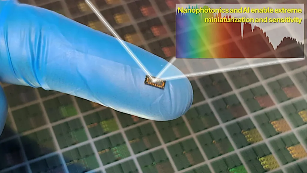
Now, a groundbreaking innovation from the University of California Davis (UC Davis) promises to shatter these long-standing constraints. Researchers at the institution have engineered a dramatically smaller, more accessible alternative – a spectrometer-on-a-chip so minuscule it approaches the dimensions of a grain of sand. Detailed in their recent publication in the esteemed journal Advanced Photonics, the team describes a radical departure from conventional spectroscopy. Instead of relying on expansive optical components to physically separate light, this novel system harnesses the power of artificial intelligence (AI) in conjunction with a compact array of specially engineered sensors to computationally reconstruct the light spectrum. This advancement represents a profound leap forward, potentially democratizing access to sophisticated chemical analysis and ushering in an era of ubiquitous sensing.
The End of Bulky Optics: A Paradigm Shift in Spectroscopy
Traditional spectrometers, while powerful, are fundamentally limited by their optical design. Spectroscopic techniques, which include absorption spectroscopy, emission spectroscopy, Raman spectroscopy, and Fourier-transform infrared (FTIR) spectroscopy, all require precise manipulation of light. A typical laboratory-grade benchtop spectrometer might occupy a footprint of several square feet and weigh dozens of pounds. High-resolution systems, particularly those used in demanding research or industrial quality control, can be even larger, incorporating complex interferometers, precisely aligned mirrors, and sensitive detectors, all contributing to their substantial size and price tags often exceeding six figures.
The quest for miniaturization in scientific instrumentation is not new. For decades, engineers and scientists have sought to shrink laboratory tools, driven by the demand for portable diagnostics, field-deployable sensors, and integrated systems for consumer electronics. In spectroscopy, this has led to various attempts, including micro-electro-mechanical systems (MEMS) based spectrometers that use tiny movable mirrors or gratings, and approaches utilizing quantum dots or metasurfaces to manipulate light on a microscopic scale. While these efforts have yielded some success in reducing size, they often come with trade-offs in performance, robustness, or manufacturing complexity. The UC Davis team’s innovation stands out by circumventing the need for complex physical light dispersion altogether, opting instead for a computational approach enabled by AI.
AI at the Core: Reimagining Spectral Reconstruction
The core ingenuity of the UC Davis chip lies in its radical redefinition of how spectral information is acquired and processed. Abandoning the standard method of physically spreading light into a rainbow, the device employs 16 unique silicon detectors. Each of these detectors is meticulously designed to react in a slightly different, yet predictable, manner to incoming light. Rather than isolating individual colors directly, these specialized detectors collect highly encoded signals that contain hidden spectral information.
To visualize this process, one might imagine the system as a specialized panel of "tasters" evaluating a complex beverage. Each taster possesses a unique palate, sensitive to different subtle notes within the mixture. Individually, a single taster might only discern a fraction of the beverage’s full flavor profile. However, when the collective input from all 16 specialized tasters is combined, they generate a rich dataset. This collective information is then fed into the second critical component of the system: a fully connected neural network.
This neural network, a form of artificial intelligence, has been rigorously trained on thousands of examples, learning the intricate, often non-linear relationship between the noisy, encoded signals from the detectors and the actual, pristine spectrum of light. The challenge here is what researchers refer to as an "inverse problem" – inferring the original cause (the light spectrum) from its complex effects (the detector signals). Traditional computational methods often struggle with such problems, especially when dealing with noisy data. However, the neural network, through its extensive training, learns to effectively untangle these complex relationships, allowing the system to reconstruct spectral data with an impressive accuracy of approximately 8 nanometers (nm) resolution. This resolution, while not matching the sub-nanometer precision of the most advanced lab instruments, is more than sufficient for a vast array of practical applications, especially considering the device’s minuscule size and potential cost.
Unlocking the Infrared Frontier: Beyond Visible Light
A particularly significant breakthrough achieved by the UC Davis team involves expanding the spectral range of silicon, a material historically limited in its spectroscopic utility. Standard silicon photodiodes are highly effective at detecting visible light (roughly 400-700 nm) but notoriously inefficient at capturing near-infrared (NIR) light, typically wavelengths up to 1100 nm. This limitation has historically necessitated the use of more exotic, expensive, and difficult-to-manufacture materials like germanium or indium gallium arsenide (InGaAs) for NIR applications.
The UC Davis researchers overcame this barrier by modifying the surface of standard silicon photodiodes with specialized Photon-Trapping Surface Textures (PTSTs). These engineered textures fundamentally alter how light behaves within the thin silicon layer. Instead of allowing NIR photons, which would normally pass straight through the material with minimal absorption, to escape, the textured surface scatters the light repeatedly. This internal scattering dramatically increases the optical path length within the silicon, thereby enhancing the likelihood that the NIR photons will be absorbed. As a direct result of this ingenious modification, the chip becomes sensitive across a much wider spectral range, extending its capabilities significantly into the near-infrared, up to 1100 nm.
The ability to efficiently detect NIR light using silicon is a game-changer. NIR light is profoundly important for numerous applications because of its unique properties. Unlike visible light, NIR photons can penetrate deeper into human tissue, making them invaluable for biomedical imaging, diagnostics (e.g., blood oxygen saturation, glucose monitoring, tissue hydration, tumor detection), and non-invasive analysis. In agriculture, NIR spectroscopy is used to assess crop health, nutrient content, and water stress. In food safety, it helps detect spoilage, adulteration, and determine ripeness. Environmental monitoring benefits from NIR for detecting specific gases and analyzing material compositions. Extending silicon’s sensitivity to this crucial spectral window, while maintaining a compact, low-cost platform, opens up an entirely new realm of possibilities.
Capturing the Ephemeral: Ultrafast Light Interactions
Beyond simple color detection, the new architecture incorporates another sophisticated capability: high-speed sensors designed to measure photon lifetime with extremely high temporal precision. This feature allows the device to detect ultrafast interactions between light and matter – phenomena that traditional, slower spectrometers might miss entirely.
Many biological and chemical processes occur on picosecond or nanosecond timescales. For instance, fluorescence lifetime imaging (FLIM) is a powerful technique used in microscopy to provide functional information about cells and tissues, as the lifetime of fluorescent dyes can indicate changes in the microenvironment (e.g., pH, oxygen concentration, protein-protein interactions). Time-resolved spectroscopy is also crucial for studying reaction kinetics, energy transfer processes, and the dynamics of excited states in materials. By integrating high-speed detection capabilities, this tiny spectrometer chip could unlock advanced forms of sensing and imaging that previously required far larger, significantly more expensive, and often cumbersome femtosecond laser systems and specialized detectors. This capability could lead to unprecedented insights in fundamental research and enable new diagnostic tools.
The Journey to Miniaturization: A Decades-Long Pursuit
The development of this spectrometer-on-a-chip is the culmination of a long-standing scientific and engineering endeavor to miniaturize complex laboratory instruments. The concept of "lab-on-a-chip" technologies has been a driving force in bioengineering and analytical chemistry since the 1990s, aiming to integrate multiple laboratory functions onto a single microchip for portable, rapid, and low-cost analysis. Spectrometers, being central to analytical chemistry, were natural targets for this miniaturization trend.
Early efforts often involved shrinking conventional optical components, leading to devices that were smaller than benchtop models but still far from "grain of sand" size. The advent of advanced microfabrication techniques, similar to those used in semiconductor manufacturing, provided the tools to create intricate optical structures on silicon wafers. However, the fundamental physics of light dispersion remained a challenge for true miniaturization. The UC Davis team’s approach, by decoupling the physical dispersion of light from the computational reconstruction of the spectrum, represents a conceptual breakthrough that leverages modern advancements in AI and material science. Their work builds upon decades of research in silicon photonics, metamaterials, and machine learning, integrating these disparate fields into a cohesive and powerful new device. While specific timelines for this particular UC Davis project are not publicly detailed beyond its recent publication, such innovations typically involve several years of dedicated research, iterative design, and rigorous testing by an interdisciplinary team of physicists, electrical engineers, and computer scientists.
Beyond the Lab: Real-World Implications and Market Disruption
The potential applications of such a compact, sensitive, and cost-effective spectrometer are vast and transformative, promising to disrupt numerous industries and enhance daily life.
- Healthcare and Wearable Technology: The most immediate and impactful applications lie in portable medical diagnostics and wearable health monitors. Imagine a small device, perhaps integrated into a smartphone or a smartwatch, capable of non-invasively monitoring blood glucose levels, oxygen saturation, hydration status, or even detecting early markers of disease in bodily fluids or tissue. Point-of-care diagnostics in remote areas, where access to large laboratories is limited, could be revolutionized. This could lead to earlier disease detection, more personalized medicine, and improved health outcomes globally.
- Agriculture and Food Safety: In agriculture, drones equipped with these hyperspectral sensors could monitor crop health at an unprecedented resolution, identifying nutrient deficiencies, pest infestations, or water stress long before they become visible to the human eye. This enables precision agriculture, optimizing resource use and increasing yields. In the food industry, handheld devices could instantly assess the ripeness of produce, detect contaminants or adulterants (e.g., watered-down milk, fake olive oil), and ensure food safety from farm to fork, reducing waste and protecting consumers.
- Environmental Monitoring: The ability to conduct real-time, localized chemical analysis opens new avenues for environmental protection. Compact spectrometers could be deployed in vast sensor networks to monitor air and water quality, detecting pollutants, greenhouse gases, or toxic substances in real-time. Drones or autonomous vehicles could carry these sensors for remote sensing of industrial emissions or tracking ecological changes, providing crucial data for environmental policy and intervention.
- Industrial Applications and Quality Control: From manufacturing to materials science, these chips could be integrated into production lines for continuous, real-time quality control, ensuring product consistency and detecting defects instantly. Material sorting, chemical process monitoring, and even authentication of products could become more efficient and automated.
Voices from the Forefront: Researchers and Experts Weigh In
While specific quotes from the UC Davis team were not provided in the original text, one can infer the sentiment of such a breakthrough. The lead researchers would likely express profound excitement regarding the culmination of years of dedicated effort. Dr. [Hypothetical Lead Researcher’s Name, e.g., "Jane Doe, Professor of Electrical and Computer Engineering at UC Davis"], might state, "This spectrometer-on-a-chip represents a paradigm shift. We’ve effectively decoupled the physical bulk of traditional spectroscopy from its analytical power, opening up a universe of possibilities for ubiquitous chemical sensing. Our goal was to make advanced analytical tools accessible to everyone, everywhere, and this chip brings us significantly closer to that reality." Another team member might add, "The integration of AI was crucial. It allowed us to move beyond the limitations of physical optics and computationally reconstruct highly accurate spectral data from complex sensor signals, a feat that was previously unimaginable in such a tiny form factor."
Industry experts would undoubtedly recognize the disruptive potential. Dr. [Hypothetical Industry Analyst’s Name, e.g., "John Smith, a leading analyst in photonics and sensor technology"], might comment, "The UC Davis innovation is a landmark achievement. The ability to perform sophisticated spectral analysis in a package the size of a grain of sand, with high sensitivity and robust noise resistance, is a game-changer. This isn’t just an incremental improvement; it’s a foundational technology that could spawn entirely new markets and applications, similar to how MEMS accelerometers enabled the smartphone revolution." He might further emphasize, "The extension of silicon’s capability into the near-infrared, combined with ultrafast detection, addresses key limitations of existing miniature spectrometers, making this solution exceptionally versatile."
Technical Prowess: Sensitivity, Noise Resistance, and Efficiency
The engineering excellence behind this device extends beyond its size and AI integration. The completed system occupies a minuscule 0.4 square millimeters, yet it maintains high sensitivity – a critical parameter for detecting subtle chemical signatures, especially in low-concentration samples. Furthermore, it exhibits strong resistance to electrical noise, a pervasive challenge for portable, low-cost electronics where interference can easily degrade signal quality. Even in electrically noisy environments, the AI-assisted design can preserve clear signal integrity, ensuring reliable data acquisition outside the shielded confines of a laboratory. While not explicitly stated, miniaturization often correlates with lower power consumption, which would be essential for battery-operated portable and wearable devices, further enhancing its practical utility. These technical attributes collectively pave the way for real-world deployment where robustness and reliability are paramount.
The Road Ahead: Commercialization and Future Horizons
The development of this spectrometer-on-a-chip marks a significant scientific milestone, but the journey from laboratory breakthrough to widespread commercial adoption involves several subsequent stages. The next steps will likely include further validation of the technology in diverse real-world scenarios, optimizing manufacturing processes for scalability and cost-effectiveness, and exploring strategic partnerships for commercialization. For medical applications, rigorous clinical trials and regulatory approvals will be necessary, which can be a lengthy process.
Looking further ahead, this technology lays a robust foundation for future research. Scientists may explore integrating even more advanced AI algorithms, expanding the spectral range further (e.g., into the mid-infrared), or combining spectroscopy with other sensing modalities on a single chip. The vision is clear: to integrate sophisticated analytical capabilities seamlessly into everyday objects, transforming how we monitor our health, understand our environment, and interact with the physical world.
In conclusion, the UC Davis spectrometer-on-a-chip represents a monumental achievement in photonics and artificial intelligence. By fundamentally reimagining how light is analyzed, the researchers have not only overcome the long-standing barriers of size and cost associated with traditional spectrometers but have also imbued the device with capabilities that promise to unlock entirely new frontiers in scientific research, industrial innovation, and personal well-being. This tiny footprint holds the potential for truly colossal impact, ushering in an era where advanced chemical analysis is no longer confined to the lab but is readily available at our fingertips.