The Engineering Dilemma: Resource Constraints in Modern Design
The fundamental problem arises when a design requires more inputs than the available silicon provides. In a recent case study involving a handheld gaming device, a developer faced the requirement of integrating six switches using only two remaining GPIO pins. Furthermore, the application necessitated the detection of simultaneous button presses—a common requirement for directional pads (D-Pads) where diagonal movement is achieved by pressing two adjacent buttons.
For developers working with microcontrollers such as the Microchip ATtiny series, the constraints are twofold. Beyond the physical pin count, these chips often possess limited flash memory, sometimes as little as 1kB or 2kB. Consequently, any solution to the pin scarcity problem must not only be hardware-efficient but also software-lean. The "cost" of a multiplexing solution is therefore measured in component count, power consumption, signal latency, and the byte-count of the driver code.
Chronology of Multiplexing Methodologies
The evolution of input expansion has seen several distinct phases, each offering different trade-offs in complexity and resource utilization.
The Era of Digital Expansion: I2C and SPI
Historically, the first recourse for an engineer running out of pins was the addition of an active integrated circuit (IC). I2C port expanders, such as the PCF8574 or MCP23017, allow for the addition of 8 to 16 GPIO pins using only two microcontroller pins (SDA and SCL). While highly scalable, this approach introduces significant overhead.
From a software perspective, an I2C solution requires a dedicated library. In a BASCOM AVR environment, for instance, implementing a basic I2C read for an 8-bit expander can consume approximately 190 bytes of flash memory. From a hardware perspective, it adds to the Bill of Materials (BOM) and requires additional PCB traces. For high-speed applications, the latency of the I2C bus (typically 100kHz to 400kHz) may also be a limiting factor.

The Shift Register Alternative
Shift registers, such as the 74HC165 for inputs or the 74HC595 for outputs, represent a more "bare-metal" approach. Traditionally requiring three pins (Data, Clock, and Latch), these can be reduced to two or even one pin using RC-delay circuits or clever bi-directional signaling. Shift registers are faster than I2C and require less flash memory because they lack the protocol overhead of device addressing. However, they remain rigid; a shift register is either an input device or an output device, lacking the flexibility of true GPIO.
Matrix Scanning and Charlieplexing
For keyboard-style inputs, matrix scanning has long been the industry standard. By arranging switches in rows and columns, $N+M$ pins can service $N times M$ switches. However, for a small number of switches, the savings are negligible. A 6-switch requirement might only be reduced from 6 pins to 5 using a $2 times 3$ matrix.
Charlieplexing, a technique famously used for LEDs, can be adapted for inputs to achieve a higher density—$N(N-1)$ switches per $N$ pins. While 3 pins could theoretically support 6 switches, Charlieplexing is notoriously difficult to implement for inputs because it requires diodes for every switch and struggles to detect simultaneous button presses without complex "ghosting" prevention logic.

Supporting Data: The Limitations of Traditional Resistive Ladders
When microcontrollers possess Analog-to-Digital Converter (ADC) capabilities, engineers often turn to resistive ladders. This method uses a single analog pin to detect multiple switches by assigning a unique voltage level to each button combination.
The traditional "parallel" resistive ladder utilizes a voltage divider where closing different switches adds resistors in parallel, altering the output voltage. However, data analysis of this configuration reveals a significant flaw: non-linearity. In a 3-switch setup using standard E12 series resistors, the voltage gaps between different button combinations can become dangerously small.
For example, a traditional ladder might produce voltages of 1.670V and 1.788V for two different states. This leaves a noise margin of only 59mV. In an environment with electromagnetic interference (EMI) or power supply fluctuations, this 59mV margin is often insufficient, leading to "phantom" button presses or failed detections. Furthermore, the code required to decode these non-linear values—usually a series of nested IF-ELSE statements—can consume upwards of 160 bytes of flash memory.

Technical Analysis: The Novel 5-Resistor Solution
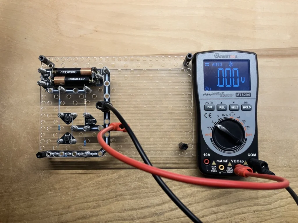
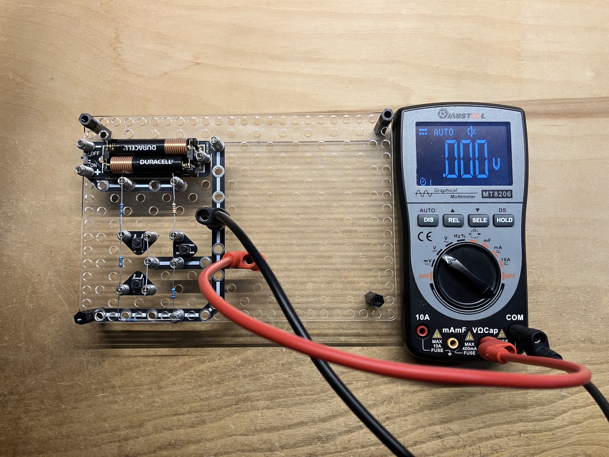
A significant breakthrough in this field involves a reconfigured resistive ladder that manipulates both the "upper" and "lower" portions of the voltage divider simultaneously. By using five resistors to service three switches on a single analog pin, the linearity of the output is vastly improved.
Comparative Performance Data:
- Standard Ladder Noise Margin: ~59mV
- Novel 5-Resistor Noise Margin: ~124mV
- Flash Memory Usage (Standard): 162 bytes
- Flash Memory Usage (Novel): 94 bytes
The primary advantage of this novel configuration is that it creates more uniform intervals between voltage states. This allows the software to use the Most Significant Bits (MSB) of the ADC value to identify the switch state. Instead of complex floating-point comparisons, the microcontroller can simply shift the ADC result and use a tiny 8-byte lookup table. This "bit-pattern" approach is significantly faster and more memory-efficient, making it ideal for the ATtiny and other low-power architectures.

The Diode Ladder: A Binary-Weighted Alternative
For applications where software simplicity is the absolute priority, the "diode ladder" offers a compelling alternative. This circuit uses the fixed forward voltage drop ($V_f$) of diodes—such as Schottky (BAS40) and Silicon (1N4148)—to create a binary-weighted voltage output.
In this setup, the 3 most significant bits of the ADC value correspond directly to the physical state of the three switches. This eliminates the need for a lookup table entirely. However, engineering analysis suggests caution regarding environmental factors. Diodes possess a temperature coefficient of approximately $-2mV/^circ C$. In extreme temperature fluctuations, the voltage levels could drift enough to cause bit-errors in the ADC reading. While compensation is possible using Negative Temperature Coefficient (NTC) resistors, this adds complexity that may negate the benefits of the diode approach in certain industrial or outdoor applications.
Broader Impact and Industry Implications
The refinement of these multiplexing techniques has broader implications for the "Right to Repair" and the "Maker" movements, as well as for commercial industrial design. By reducing the number of pins required for complex user interfaces, designers can utilize smaller, cheaper, and more available microcontrollers. During the global semiconductor shortages of recent years, the ability to port a design from a high-pin-count chip to a more readily available low-pin-count variant became a critical survival strategy for many manufacturers.

Furthermore, the reduction in flash memory requirements supports the trend toward "minimalist computing," where efficient code allows for longer battery life and reduced thermal output. In the consumer electronics sector—particularly in remote controls, handheld toys, and simple medical devices—the ability to save even $0.10 per unit by using a smaller MCU and a few cents worth of resistors can result in millions of dollars in savings over a product’s lifecycle.
Conclusion: The Future of Resource-Constrained Design
As the industry pushes toward the "Internet of Everything," the demand for ultra-low-cost, high-efficiency input solutions will only grow. The transition from complex digital ICs back to clever analog resistor configurations represents a full circle in engineering logic: using the fundamental laws of physics to solve problems that software alone cannot.
While digital expanders will always have a place in high-complexity systems, the novel resistive solutions discussed here prove that ingenuity in circuit design can overcome the physical limitations of silicon. For the modern engineer, the goal remains unchanged: to extract the maximum possible utility from the minimum possible resources, ensuring that even the humblest microcontroller can handle the complexities of modern human-machine interaction.