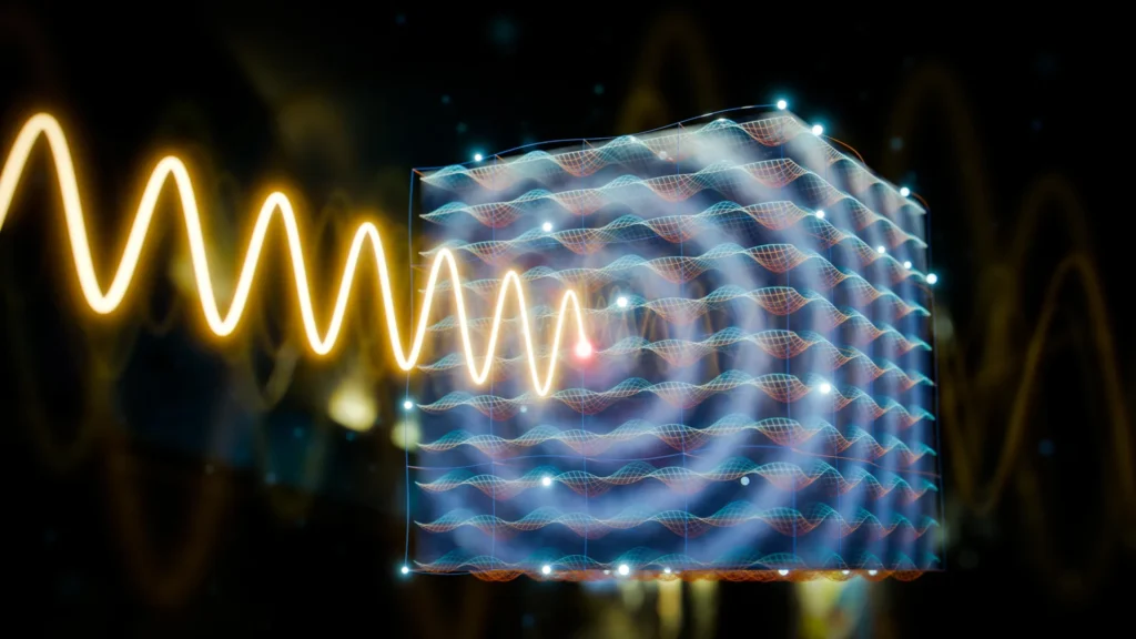
An international collaborative research team has achieved a significant scientific milestone, experimentally producing the world’s first all-optical photonic time crystal (PTC). This groundbreaking material is specifically engineered to dynamically alter its optical behavior with unprecedented speed and repeatability over time, representing a paradigm shift in how light can be manipulated. The pioneering work involved researchers from prominent European institutions, including École Polytechnique in France, Collège de France, and the Helmholtz-Zentrum Dresden-Rossendorf (HZDR) in Germany, underscoring the collaborative nature of cutting-edge scientific discovery. This monumental achievement, detailed in the prestigious scientific journal Nature, promises to unlock new capabilities in fields ranging from computing and telecommunications to advanced laser technology.
The Dawn of Dynamic Light Control
The ability to precisely control the propagation and interaction of light within various materials has been a cornerstone of modern technological advancement. Technologies such as fiber optics, which underpin global communication networks by guiding light signals across vast distances, and highly precise lasers, indispensable in manufacturing, medicine, and scientific research, are direct outcomes of this mastery. Optical sensors, widely deployed in chemical analysis and biological diagnostics, further illustrate the transformative power of engineered light-matter interactions. These existing technologies primarily rely on materials with fixed spatial arrangements that dictate light’s behavior. The concept of a photonic time crystal, however, introduces a revolutionary dimension: manipulating light’s properties not just through static spatial patterns but through dynamic, time-varying changes in the material itself.
Bridging the Terahertz Gap: A New Frontier
A critical enabler for this breakthrough was HZDR’s formidable TELBE superradiant terahertz source. This state-of-the-art facility provided the researchers with an unparalleled platform to explore a previously inaccessible regime of light-matter interaction within the terahertz (THz) frequency range. The terahertz spectrum, often referred to as the "terahertz gap," occupies a unique and largely underexplored segment of the electromagnetic spectrum, positioned precisely between conventional electronics and photonics. This region, characterized by frequencies 1,000 times faster than those typically utilized in electronic components, holds immense promise for developing new methods to examine, control, and manipulate matter at ultrafast timescales.
Yannis Laplace, an assistant professor and leader of a research team at the Laboratory of Irradiated Solids (LSI) at École Polytechnique, has been at the forefront of developing photonic devices capable of controlling light in this challenging THz frequency range. "The THz range represents the frontier between electronic and photonic technologies," explains Laplace. "It is a range full of opportunities both for science and for society, yet is still underdeveloped technologically compared to its electrical and photonic counterparts. Creating photonic crystals could lead the way to the closing of this gap." The potential applications of mastering the terahertz range are vast, spanning from high-speed wireless communication and advanced security imaging to novel medical diagnostics and fundamental studies of material properties.
From Static Lattices to Temporal Patterns
To appreciate the significance of a photonic time crystal, it’s essential to understand its conventional counterpart: the photonic crystal. Traditional photonic crystals are meticulously nanostructured materials featuring a repeating optical pattern, akin to an atomic lattice. This intricate arrangement dictates how photons traverse the material. By carefully designing and arranging materials with distinct shapes and refractive indices, scientists can precisely block, guide, or enhance specific wavelengths of light. In essence, these crystals control photons in a manner analogous to how semiconductors regulate the flow of electrons, forming the basis of modern electronics.
Earlier investigations by Laplace’s team had already demonstrated that factors such as temperature and external magnetic fields could influence the light-capturing capabilities of photonic crystals. However, a fundamental limitation persisted: once these external conditions were established, the optical behavior of the crystal remained static and fixed over time. The innovative photonic time crystal developed by the international team transcends this limitation. Its optical properties, including reflectivity and resonance frequency, can be dynamically altered on picosecond timescales—an incredibly brief duration, approaching the timescale of light’s own oscillations. This innovation moves beyond merely relying on patterns arranged across space, instead introducing a repeating pattern in time, fundamentally redefining light control.
Tingwen Guo, a PhD student at École Polytechnique and the lead author of the publication, emphasizes the profound implications of this advancement. "By extending photonic crystals from space to time, we open a new dimension for light control – and a novel path toward amplification and lasing. That could be a game-changer for optical technologies at terahertz frequencies and beyond," Guo states, highlighting the potential for entirely new optical functionalities and device designs.
Engineering the Photonic Time Crystal
The realization of such rapid and precise control necessitated the development of a highly specialized and complex device. With crucial support from Thales’ Laboratoire Albert Fert and Polytechnique’s Physics of Interfaces (PICM) laboratory, the researchers meticulously constructed a novel form of photonic crystal known as a "plasmonic metamaterial." Metamaterials are artificially engineered materials designed to possess properties not found in nature, often by structuring them at scales smaller than the wavelength of light they interact with.
The core of this advanced material comprises micrometer-scale gold crenelated structures. These intricate gold patterns are precisely positioned above an insulating layer, which in turn sits atop a semiconductor composed of a carefully balanced mixture of indium and antimony. The gold structures are designed to form tiny cavities that effectively confine light between the gold layer and the underlying semiconductor. When the semiconductor surface is excited, it generates "surface plasmons"—collective oscillations of electrons that propagate along the interface. These surface plasmons possess a remarkable ability to capture light and sustain its oscillations, providing the researchers with a powerful mechanism to manipulate the trapped photons with exceptional speed and precision. This intricate interplay between the metallic nanostructures and the semiconductor forms the foundation of the photonic time crystal’s dynamic capabilities.
The Power of TELBE: Enabling Ultrafast Modulation
The experimental validation of the photonic time crystal’s capabilities involved exposing the device to intense terahertz laser pulses generated by the TELBE facility at HZDR’s ELBE accelerator. TELBE stands out as a unique infrastructure capable of generating high-field, phase-stable terahertz pulses. Its ability to produce intense terahertz radiation, coupled with the flexibility to tune these pulses to different frequencies, proved indispensable. This allowed the researchers to induce strong and rapid changes in the material’s optical properties, particularly its reflectivity.
Achieving both the strength and the speed of these changes simultaneously had previously represented a significant technical hurdle in the field. The magnitude of the observed change in optical properties was remarkable, comparable to forcing an object to emit a completely different color, while the transformation itself occurred on a picosecond scale—an astonishingly short duration equivalent to one billionth of a billionth of a second (10^-12 seconds). Such ultrafast, strong modulation is a hallmark of the photonic time crystal concept.
Jan-Christoph Deinert, the coordinator of the TELBE facility, underscored the critical role of the infrastructure. "TELBE’s unique ability to generate high-field, phase-stable terahertz pulses was critical," confirmed Deinert. "Without this infrastructure, achieving the coherent, ultrafast modulation needed for the PTC regime would have been impossible." This highlights the synergy between cutting-edge material science and advanced experimental facilities in pushing the boundaries of scientific discovery.
Theoretical Foundation and Dissipation Reduction
Complementing the experimental findings, a robust theoretical model was developed by Marco Schirò, a Research Scientist at Collège de France, and his dedicated team. This model not only supported the observed experimental results but also provided invaluable insights into the intricate behavior of photons within the novel device. The theoretical calculations offered a deeper understanding of the underlying physical mechanisms governing the photonic time crystal’s operation.
A particularly significant revelation from the theoretical work was that dynamically changing the material’s properties over time effectively reduced photon dissipation by half. In this context, photon dissipation refers to the portion of photons that are not reflected by the metamaterial’s surface and instead pass through or are absorbed. Minimizing dissipation is crucial for enhancing the efficiency and performance of optical devices. "The theory not only reproduces the experiment but also provides the basis for guiding future discoveries in this system," rejoiced Schirò, emphasizing the model’s predictive power and its role in charting the course for subsequent research efforts. This strong agreement between theory and experiment validates the fundamental principles behind photonic time crystals and provides a solid foundation for future development.
Future Horizons: Revolutionizing Optical Technologies
The successful experimental realization of the all-optical photonic time crystal marks a pivotal moment in photonics research, but the journey of discovery is far from over. The research team is now focused on several key objectives to further enhance the device’s performance and unlock its full potential. Foremost among these goals is to further reduce photon dissipation and significantly increase the number of photons that can be effectively held and manipulated within the crystal. If these efforts succeed in producing sufficiently strong amplification, the current device could evolve into the foundational element for highly adaptable and powerful new lasers, operating with unprecedented speed and tunability.
The implications of photonic time crystals could ultimately reshape how light is harnessed and utilized across a broad spectrum of technological applications, particularly within the promising terahertz range. Their unparalleled ability to dynamically alter light on extremely short timescales could underpin a new generation of ultrafast lasers, with transformative potential for applications such as high-resolution medical imaging, where speed and precision are paramount, and next-generation telecommunications, enabling vastly increased data transmission rates.
Moreover, this innovative technology may facilitate the instantaneous and on-demand tuning of crucial light properties, such as its "color" (wavelength or frequency) or intensity. Such a degree of granular, dynamic control over light opens the door to the development of optical systems that are not only significantly faster and smarter but also far more adaptable to diverse and evolving technological demands. From ultra-secure quantum communications to advanced sensing platforms and potentially even the architecture of future ultrafast optical computers, the all-optical photonic time crystal stands as a testament to scientific ingenuity, promising to illuminate new pathways for technological innovation in the 21st century.