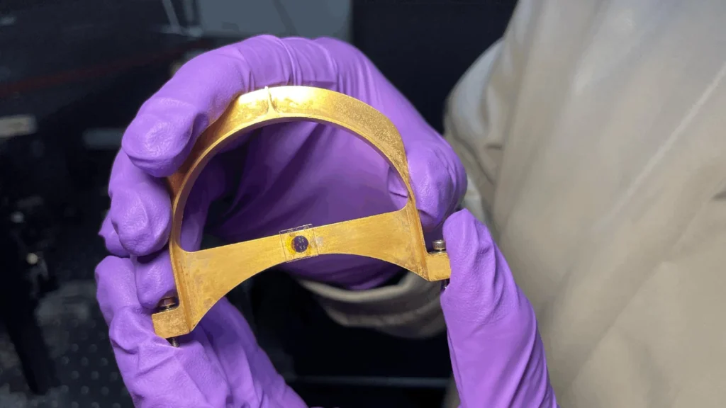
Quantum computers today are notoriously difficult and expensive to operate, demanding temperatures near absolute zero—approximately -459 degrees Fahrenheit—to preserve the incredibly fragile quantum states essential for computation and communication. This extreme cryogenics represents one of the most significant barriers to the widespread adoption and practical application of quantum technologies. However, a recent and transformative development from Stanford University may signal a profound shift in this landscape. Researchers there have engineered a nanoscale optical device that functions effectively at room temperature, crucially linking the quantum properties of light and electrons. This pioneering advance promises to dramatically reduce the size, cost, and complexity of future quantum technologies, particularly those geared towards transmitting information across vast distances.
The newly developed device represents a critical leap forward, enabling stable entanglement between photons, the fundamental particles of light, and electrons. This intricate quantum connection is universally recognized as a foundational requirement for the sophisticated quantum communication systems of tomorrow. Jennifer Dionne, a professor of materials science and engineering at Stanford and the senior author of the groundbreaking study published in Nature Communications, emphasizes the novel approach taken by her team. "The material in question is not really new, but the way we use it is," Dionne explains. "It provides a very versatile, stable spin connection between electrons and photons that is the theoretical basis of quantum communication. Typically, however, the electrons lose their spin too quickly to be useful." This ability to maintain electron spin, a crucial quantum property, at ambient temperatures for long enough to be useful marks a significant departure from conventional methods.
The Quantum Conundrum: A Cold and Costly Frontier
For decades, the pursuit of quantum technologies has been hampered by a fundamental paradox: to harness the delicate and counter-intuitive phenomena of the quantum world, researchers have largely had to isolate quantum systems from the classical world’s thermal noise. This isolation usually entails supercooling materials to temperatures colder than deep space, often just a few millikelvin above absolute zero. The infrastructure required for such extreme refrigeration is monumental, involving multi-stage dilution refrigerators, complex vacuum systems, and extensive shielding to protect qubits from environmental interference. These setups are not only physically enormous, often filling entire laboratories, but also astronomically expensive, with cryogenic equipment alone costing millions of dollars. Furthermore, the energy consumption associated with maintaining these ultra-low temperatures is substantial, adding to the operational overhead. This "cold and costly" reality has confined quantum computing and communication to specialized research facilities, limiting scalability and accessibility. The dream of a practical, ubiquitous quantum internet or a personal quantum device has remained largely theoretical due to these formidable engineering challenges.
Bridging the Quantum Divide: The Stanford Innovation
The Stanford device directly addresses this central challenge. At its core, the innovation lies in combining a thin, precisely patterned layer of molybdenum diselenide (MoSe2) with a nanopatterned silicon substrate. Molybdenum diselenide is a member of the family of materials known as transition metal dichalcogenides (TMDCs), which have garnered intense interest in recent years due to their extraordinary optical and quantum properties. These two-dimensional materials possess unique electronic and optical characteristics, including strong light-matter interaction and direct bandgaps, making them ideal candidates for quantum applications.
According to the researchers, the silicon nanostructures are not merely a substrate but play a pivotal and active role by generating what they term "twisted light." Feng Pan, a postdoctoral scholar in Dionne’s lab and the paper’s first author, elaborates on this ingenious mechanism. "The Silicon nanostructures enable what we call ‘twisted light,’" Pan explains. "The photons spin in a corkscrew fashion, but more importantly, we can use these spinning photons to impart spin on electrons that are the heart of quantum computing." This transfer of orbital angular momentum (OAM) from photons to electrons’ intrinsic spin is the lynchpin of the device’s functionality. The patterned structures themselves are incredibly minute, roughly comparable in size to the wavelength of visible light and utterly invisible to the naked eye. Dionne adds, "The patterned nanostructures are imperceptible to the human eye, about the size of the wavelength of visible light. But they help us manipulate photons very precisely to make them spin — to twist them — in a specific direction, for example, up or down." This precise control over photon OAM is what allows for the efficient and stable transfer of quantum information to electron spins.
The Ingenuity of "Twisted Light" and Electron Spin
To appreciate the significance of "twisted light," it’s important to understand the concept of orbital angular momentum (OAM) in photons. Unlike spin angular momentum, which describes the polarization of light, OAM describes the helical or "corkscrew" wavefront of a photon. Photons carrying OAM are often described as "twisted" because their phase front spirals around the direction of propagation. This property can be used to encode information, adding another dimension to quantum communication. The silicon nanostructures designed by the Stanford team are engineered to specifically generate and manipulate these twisted photons. When light interacts with these precisely crafted nanostructures, it acquires OAM.
The genius of the Stanford device lies in how it leverages this twisted light. By carefully designing the interaction between these OAM-carrying photons and the MoSe2 material, the researchers are able to efficiently transfer the angular momentum from the photons to the electrons within the MoSe2. This transfer imparts a specific spin state to the electrons, effectively creating a qubit – the basic unit of quantum information. The challenge with electron spins is their susceptibility to decoherence, where external noise causes them to lose their delicate quantum state. The MoSe2, combined with the precise interaction enabled by the twisted light, creates an environment where these electron spins can maintain their coherence for a sufficiently long duration at room temperature. This robust and stable coupling between photon OAM and electron spin is what differentiates this breakthrough, offering a novel pathway to creating stable, addressable qubits without the need for extreme cooling.
Qubits, Entanglement, and the Challenge of Decoherence
In conventional computing, information is encoded as bits, which can be either 0 or 1. Quantum technologies, however, utilize qubits, which can exist in a superposition of both 0 and 1 simultaneously. This property, along with entanglement – where two or more qubits become inextricably linked, sharing the same fate regardless of distance – allows quantum systems to process and transmit information in fundamentally new and powerful ways. The ability to entangle photons and electrons is paramount for quantum communication. Photons are excellent carriers of quantum information over long distances, but they don’t interact strongly with each other, making storage and processing difficult. Electrons, with their spin states, are ideal for local quantum memory and processing but are less suitable for long-distance transmission. A device that can reliably entangle photons and electrons acts as a crucial interface, allowing quantum information to be transferred between a flying qubit (photon) and a stationary qubit (electron).
One of the biggest obstacles facing quantum technologies, and a primary reason for the need for extreme cooling, is maintaining stable quantum states against decoherence. Decoherence is the process by which delicate quantum information is lost due to interaction with the environment. Even the slightest vibration, stray electromagnetic field, or thermal fluctuation can cause a qubit to lose its superposition or entanglement, collapsing its quantum state into a classical one. In many existing quantum systems, extreme cooling is necessary to suppress thermal energy and minimize environmental interactions, thus prolonging the coherence time of qubits. Because the new Stanford device operates at room temperature, it bypasses one of the major engineering and cost obstacles that has historically limited the widespread development and use of quantum technologies. The researchers also highlight the compact and nanoscale design, which is inherently more inexpensive and practical compared with the sprawling, cryogenically dependent systems currently in use.
The Material Matters: Molybdenum Diselenide and TMDCs
The selection of molybdenum diselenide (MoSe2) was a deliberate and critical choice. The team specifically chose TMDC materials due to their unusual quantum characteristics, collaborating with Stanford researchers Fang Liu and Tony Heinz, who are specialists in these advanced materials. TMDCs are a class of two-dimensional materials, similar to graphene, but with distinct electronic and optical properties. They often possess a direct bandgap, which means they can efficiently absorb and emit light, a crucial feature for optoelectronic and quantum applications. Furthermore, TMDCs exhibit strong spin-orbit coupling and spin-valley locking, which means that an electron’s spin state is intrinsically linked to its momentum valley in the material’s band structure. This property makes them particularly attractive for encoding and manipulating quantum information via electron spin.
Pan underscores the synergy between the materials: "It all comes down to this material and our Silicon chip. Together, they efficiently confine and enhance the twisting of light to create a strong coupling of spin between photons and electrons. This stabilizes the quantum state that makes quantum communication possible." The combination of the atomically thin MoSe2, with its inherent quantum properties, and the precisely engineered silicon nanostructures, which control the optical environment, allows for an unprecedented level of light-matter interaction. This strong coupling helps to preserve the fragile quantum properties — specifically the electron spin — needed for robust communication and future computing tasks, even at ambient temperatures. This material-by-design approach highlights the growing importance of advanced materials science in pushing the boundaries of quantum technology.
A Simpler Path to Quantum Communication and Beyond
The immediate and most profound implication of this room-temperature entanglement device lies in quantum communication. Researchers can leverage this twisted light to become entangled with electron spins, effectively creating stable qubits that can interface between photonic channels and electron-based memory. This is a fundamental building block for future quantum information systems. Current quantum communication protocols, such as Quantum Key Distribution (QKD), rely on sending individual photons over optical fibers. However, losses in fibers limit distances, and "quantum repeaters" are needed to extend the range. These repeaters require local quantum memory capable of storing and processing entangled states. A room-temperature, compact device capable of entangling photons and electrons could form the core of such repeaters, significantly simplifying their design and deployment.
If further developed and scaled, this technology could contribute to monumental advances in several critical areas. In secure communications, it could enable truly unhackable quantum networks, safeguarding sensitive data for governments, financial institutions, and individuals. In advanced sensing, stable room-temperature qubits could lead to ultra-precise sensors for medical diagnostics, navigation, and environmental monitoring. For high-performance computing, while primarily a communication breakthrough, the ability to maintain quantum coherence at room temperature could pave the way for more practical hybrid quantum-classical computing architectures. Moreover, emerging fields like artificial intelligence stand to benefit from quantum acceleration, with algorithms potentially performing complex tasks far more efficiently. The compact and relatively inexpensive design, compared to existing cryogenic systems, makes these applications far more tangible.
Chronology of Research and Future Trajectories
The development of this device is the culmination of years of foundational research in materials science and quantum optics. The journey involved:
- Early 2010s: Intensified research into 2D materials like TMDCs, recognizing their unique electronic and optical properties for next-generation electronics and photonics.
- Mid-2010s: Growing interest in using OAM of light for quantum information encoding and manipulation, alongside efforts to understand and control electron spins in semiconductors.
- Late 2010s: Focused efforts at Stanford and elsewhere on integrating TMDCs with photonic nanostructures to enhance light-matter interaction and explore quantum phenomena at room temperature.
- Early 2020s: Specific research at Dionne’s lab on designing silicon nanostructures to generate twisted light and investigating its interaction with TMDCs to achieve stable spin-photon entanglement.
- 2024: Publication of the Nature Communications study, announcing the successful demonstration of a room-temperature nanoscale device linking quantum properties of light and electrons.
Looking ahead, the researchers are not resting on their laurels. They are actively working to refine and improve the device’s performance. This includes exploring additional TMDC materials and novel material combinations that could deliver even better efficiency, longer coherence times, and higher entanglement fidelity. They are also investigating whether these novel systems might unveil entirely new quantum capabilities that are not currently feasible at room temperature, potentially leading to unforeseen applications.
A more ambitious, longer-term goal is the seamless integration of devices like this into larger, robust quantum networks. Achieving this grand vision will necessitate concurrent improvements in a host of supporting technologies, including more efficient quantum light sources, high-speed modulators for encoding information, ultra-sensitive detectors for reading out quantum states, and scalable interconnects to link various quantum components. The field of quantum technology is a complex ecosystem, and progress in one area often catalyzes advancements in others.
Broader Impact and Implications: Towards a Quantum Future
The implications of this Stanford breakthrough extend far beyond the laboratory. While the quantum technology market is still nascent, it is projected to grow significantly, with some estimates placing its value in the tens of billions of dollars within the next decade. Major players, from tech giants like IBM, Google, and Microsoft to government agencies and defense contractors, are investing heavily in quantum research, recognizing its potential to revolutionize computing, communication, and sensing. A practical, room-temperature quantum device capable of entangling photons and electrons would be a tremendous boon to this burgeoning industry. It could democratize access to quantum capabilities, moving beyond the highly specialized and capital-intensive environments currently required.
This development could accelerate the timeline for realizing a functional quantum internet, enabling secure communication resistant to even the most powerful future classical computers. It could also spur the creation of new types of quantum sensors that are more compact and deployable outside of highly controlled lab settings. While the immediate focus is on communication, the fundamental ability to manage quantum states at room temperature has downstream effects on quantum computing, potentially allowing for hybrid architectures that leverage classical processing with quantum co-processors that are easier to integrate.
Ultimately, the vision is to miniaturize quantum components to a degree where they could be incorporated into everyday electronics. While that future remains many years, if not decades, away, the work from Stanford represents a concrete and significant step toward making quantum technology more accessible, practical, and ubiquitous. As Pan muses with an optimistic smile, "If we can do that, maybe someday we could do quantum computing in a cell phone. But that’s a 10-plus-year plan." This breakthrough, therefore, is not just a scientific achievement; it’s a vital milestone on the long, complex, but increasingly promising road to a truly quantum-enabled world.