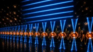
Researchers at the California Institute of Technology (Caltech) have announced a transformative development in the field of integrated photonics, successfully demonstrating a method to move light across silicon wafers with unprecedented efficiency. By achieving signal loss levels at visible wavelengths that approach the performance of high-purity optical fiber, the team has bridged a long-standing gap between long-haul telecommunications technology and chip-scale microelectronics. This innovation, detailed in a recent publication in the journal Nature, paves the way for a new class of photonic integrated circuits (PICs) characterized by high coherence and extreme energy efficiency. These circuits are expected to revolutionize a broad spectrum of industries, from AI-driven data center communications and quantum computing to the development of ultra-precise optical clocks and navigational gyroscopes.
The Convergence of Fiber Purity and Chip-Scale Manufacturing
For decades, the backbone of global communication has relied on optical fiber—thin strands of glass capable of carrying vast amounts of data over thousands of kilometers. The secret to the success of optical fiber lies in the extreme purity of the glass and the engineered smoothness of its surfaces, which allow light to travel with "ultralow loss." In contrast, integrating these same capabilities onto a silicon chip—the standard platform for modern computing—has proven notoriously difficult.
While silicon photonics has made significant strides in the infrared spectrum, visible light has remained a challenge. Standard chip-scale materials often absorb or scatter visible light, leading to significant signal degradation. The Caltech team, led by Kerry Vahala, the Ted and Ginger Jenkins Professor of Information Science and Technology and Applied Physics, sought to resolve this by essentially "printing" the material properties of optical fiber directly onto the silicon wafers used in traditional semiconductor manufacturing.
The significance of this transition cannot be overstated. By moving toward fiber-like performance on 8- and 12-inch wafers, the researchers are enabling the mass production of optical circuits that benefit from negligibly low energy loss. This shift is critical as the global demand for bandwidth and processing power continues to surge, particularly in the realm of artificial intelligence.
Technical Innovation: The Germano-Silicate Platform
The breakthrough centers on the use of germano-silicate, a type of glass identical to that found in high-end optical fibers. Traditionally, this material was difficult to adapt to the lithography-based manufacturing processes required for chip fabrication. However, the Caltech team developed a method to create waveguides—nanoscale pathways that channel light—using this glass on standard silicon wafers.
To maximize the efficiency of these waveguides, the researchers employed a spiral architecture. Rather than directing light in straight lines, which would require a massive physical footprint to achieve significant path lengths, they arranged the waveguides in tight, microscopic spirals. This design allows light to travel a long optical path while remaining confined within a very small area on the chip. This mimics the effect of winding kilometers of optical fiber around a spool but does so at a scale compatible with microchips.
A critical component of the manufacturing process involves a "reflow" technique. Because germano-silicate has a relatively low melting temperature compared to other chip-making materials, the researchers can place the finished wafers into a furnace to slightly melt, or reflow, the surface of the waveguides. This process smooths the surface down to the level of individual atoms, effectively eliminating the surface roughness that typically causes light to scatter. This atomic-level smoothness is the primary driver behind the 20-fold improvement in performance observed at visible wavelengths compared to silicon nitride, the previous industry standard.
Comparative Data and Performance Benchmarks
The performance of the new germano-silicate platform was tested against silicon nitride, which has long been the preferred material for low-loss photonic circuits due to its transparency across a wide range of wavelengths.
At near-infrared wavelengths—the spectrum used for most current fiber-optic telecommunications—the Caltech platform matched the performance of the most advanced silicon nitride devices. However, the true advantage emerged in the visible light spectrum (ranging from violet to red). In these bands, the germano-silicate waveguides exhibited losses 20 times lower than the best-recorded silicon nitride circuits.
The implications of reducing loss extend beyond merely keeping the light "bright." In photonics, lower loss directly translates to higher coherence. The researchers reported that lasers integrated into this new platform showed a 100-fold improvement in coherence over previous designs. Coherence refers to the "purity" of the light wave and its ability to remain in phase over time, a metric that is vital for precision measurements and high-speed data encoding.
Impact on AI Data Centers and Energy Efficiency
One of the most immediate applications for this technology lies in the infrastructure of modern data centers. As AI models grow in complexity, the energy required to move data between servers has become a significant bottleneck and environmental concern.
Henry Blauvelt, a visiting associate at Caltech and Chief Technology Officer at Emcore, emphasized that the germano-silicate waveguides are highly efficient at transferring light between optical fibers and semiconductor lasers. This "coupling efficiency" is paramount for reducing the total energy cost of server infrastructure. By minimizing the power lost as light enters and exits the chip, data centers can operate with significantly lower thermal outputs and electrical requirements.
In a landscape where energy consumption by data centers is projected to account for an increasing percentage of global electricity usage, the ability to integrate ultralow-loss optical paths directly onto server chips offers a sustainable path forward for the expansion of cloud computing and AI training.
Scientific and Quantum Applications: From Atomic Clocks to Ion Traps
Beyond the commercial sector, the ability to manipulate visible light with such precision opens new doors in fundamental science. Many atomic and molecular operations—such as those required for atomic clocks and quantum sensors—occur at visible or ultraviolet wavelengths.
Hao-Jing Chen, a postdoctoral scholar at Caltech and lead author of the study, noted that the expanded wavelength coverage would support chip-scale atomic sensors and ion-trap systems. Ion traps, which are a leading candidate for building functional quantum computers, require precisely controlled visible light to manipulate individual atoms. Currently, these systems often rely on bulky, "table-top" laser setups. The Caltech breakthrough suggests that these complex systems could eventually be shrunk down to the size of a handheld chip without sacrificing the performance required for quantum gates.
Furthermore, the technology enables the creation of high-performance ring resonators. These devices circulate light in a loop, strengthening it at specific frequencies. In the new germano-silicate platform, light can circulate for much longer periods, meaning a physical ring only a few millimeters in diameter can have an "effective" optical path length measured in meters or even kilometers. This capability is essential for developing the next generation of gyroscopes for navigation and ultra-stable clocks for GPS-independent timing.
Chronology of Development and Collaborative Efforts
The current results represent the culmination of over five years of intensive research within Kerry Vahala’s lab. The project began with the goal of translating the established benefits of "spool-based" fiber optics into the realm of "wafer-based" semiconductor manufacturing.
- 2019-2021: Initial experimentation with germano-silicate deposition on silicon. The team focused on overcoming the material stresses that typically cause glass films to crack when applied to silicon wafers.
- 2022: Development of the spiral waveguide architecture and the initial refinement of the "reflow" process to reduce scattering loss.
- 2023: Testing phase across the visible spectrum, where the 20-fold advantage over silicon nitride was first documented.
- 2024: Publication of the findings in Nature and demonstration of integrated devices including lasers and nonlinear resonators.
The research was a highly collaborative effort, involving experts from across the globe. Key contributors included researchers from UC Santa Barbara, Leiden University in the Netherlands, and the University of Southampton in the United Kingdom. The project was supported by several high-profile agencies, including the Defense Advanced Research Projects Agency (DARPA) and the Air Force Research Laboratory (AFRL), highlighting the strategic importance of ultralow-loss photonics for national security and defense.
Future Outlook: Scaling Toward Mass Production
While the current results are groundbreaking, the researchers view this as an ongoing journey. Professor Vahala remarked that while they have made significant progress, there is still "room to improve." The next phase of research will likely focus on further reducing losses in the ultraviolet spectrum and finding ways to integrate these photonic circuits with existing electronic components on the same chip—a concept known as monolithic integration.
The move to 8- and 12-inch wafers is particularly significant because these are the standard sizes used by commercial semiconductor foundries like TSMC and Intel. This compatibility suggests that the transition from laboratory success to industrial application could be relatively swift. As the technology matures, it could lead to a paradigm shift in how we build computers, moving away from purely electronic circuits toward "hybrid" chips that use electrons for logic and photons for communication and sensing.
The Caltech team’s work effectively brings the "gold standard" of telecommunications—the optical fiber—down to the microchip level. In doing so, they have provided the tools necessary to build a faster, more precise, and more energy-efficient digital future. Whether through the lens of a quantum computer or the backbone of an AI data center, the "Swiss Army-knife" of germano-silicate photonics is set to become a cornerstone of next-generation technology.