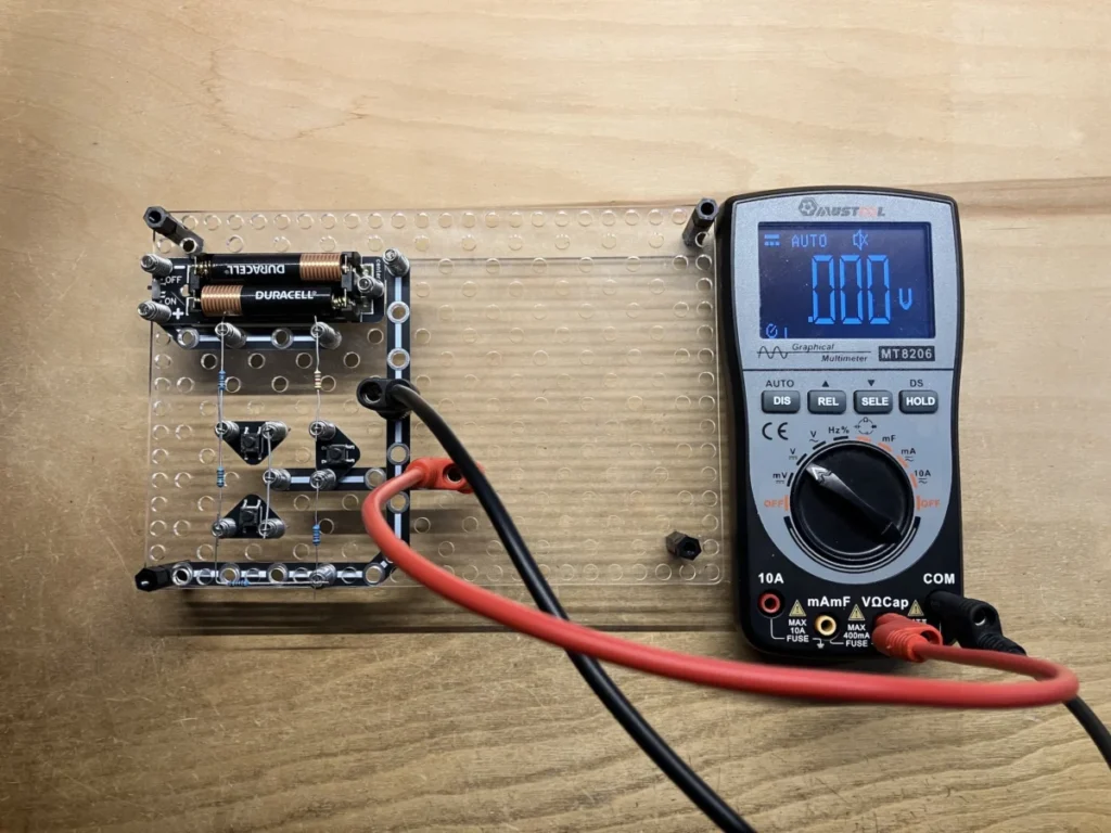
The persistent challenge of pin scarcity in microcontroller-based system design has long forced engineers and hobbyists alike to navigate a complex trade-off between hardware complexity, cost, and code efficiency. As the demand for smaller, more integrated handheld devices grows, the limitations of popular low-power microcontrollers, such as the ATtiny series, become increasingly apparent. These chips often feature as few as six to eight pins, several of which are reserved for power, ground, and reset functions, leaving a meager selection of General Purpose Input/Output (GPIO) pins for user interfaces. When a project requires multiple tactile inputs—such as a directional pad (D-Pad) and action buttons—the "GPIO wall" is reached almost immediately.
Recent developments in circuit design, highlighted by engineer Chris Wasshuber, have introduced novel methods for multiplexing inputs that significantly outperform traditional resistive ladders and integrated circuit (IC) solutions. By focusing on maximizing noise margins and minimizing flash memory overhead, these techniques offer a path forward for high-performance applications on ultra-constrained hardware.
The Evolution of Input Expansion: A Technical Chronology
The history of input expansion in digital electronics has transitioned from discrete logic gates to sophisticated serial protocols. In the early eras of computing, input expansion was typically handled through parallel bus architectures. However, as microcontrollers moved toward miniaturization, serial communication became the standard.
The Rise of I2C and Serial Port Expanders
By the 1990s, the Inter-Integrated Circuit (I2C) protocol, developed by Philips Semiconductor, became the industry standard for peripheral communication. Chips like the PCF8574 or the MCP23017 allowed designers to add 8 to 16 GPIO pins using only two microcontroller pins (SDA and SCL). While highly effective for large-scale systems, the I2C approach introduces significant overhead. A standard software-implemented I2C library can consume nearly 200 bytes of flash memory—a substantial portion of the 1kB total found in chips like the ATtiny13. Furthermore, the communication speed is limited by the I2C bus clock (typically 100kHz or 400kHz), which may introduce latency in time-sensitive gaming or control applications.
Shift Registers and Pin Reduction
The use of shift registers, such as the 74HC165 for inputs and 74HC595 for outputs, provided a faster, more memory-efficient alternative. These chips operate on a synchronous serial interface requiring three pins: data, clock, and latch. While techniques exist to reduce this to one or two pins using RC-delay circuits, the requirement for an external IC remains. In the context of modern surface-mount technology (SMT) design, adding an extra chip increases the Bill of Materials (BOM) cost and consumes valuable PCB real estate.

Traditional Multiplexing Strategies and Their Limitations
Before the advent of specialized analog techniques, designers relied on two primary geometric configurations: the Matrix and Charlieplexing.
Matrix Scanning
In a matrix configuration, switches are arranged in rows and columns. A 3×3 matrix can support nine switches using six pins. While efficient for larger arrays, the "savings" are negligible for small-scale interfaces. For instance, managing six switches in a 2×3 matrix requires five pins—only a one-pin saving over direct connection. Additionally, matrices suffer from "ghosting" when three or more buttons are pressed simultaneously, necessitating the addition of blocking diodes.
Charlieplexing
Named after Charlie Allen of Maxim Integrated in 1995, Charlieplexing leverages the tri-state logic of microcontroller pins (High, Low, and High-Impedance). While famous for driving LEDs, it is rarely used for inputs because it cannot reliably detect simultaneous button presses. For a handheld device where a user might press "Up" and "Left" simultaneously for diagonal movement, Charlieplexing is fundamentally unsuitable.

The Analog Shift: Resistive Ladders and ADC Decoding
The most promising avenue for pin-constrained devices is the use of Analog-to-Digital Converters (ADCs). By associating different switch combinations with specific voltage levels, a single analog pin can theoretically monitor dozens of inputs.
The Standard Resistive Ladder
The traditional approach involves a parallel resistive ladder forming a voltage divider. In a three-switch configuration, resistors are added in parallel as buttons are pressed, altering the voltage read by the ADC.
However, this method faces two critical flaws:

- Non-Linearity: The resulting voltages do not follow a linear progression, leading to "crowding" at certain parts of the voltage range.
- Narrow Noise Margins: Using standard E12 series resistors (the common 10, 12, 15… sequence), the gap between different button states can be as small as 59mV. In an environment with electromagnetic interference (EMI) or power supply fluctuations, this can lead to "phantom" button presses.
Breaking the Efficiency Barrier: The Wasshuber Novel Resistive Solution
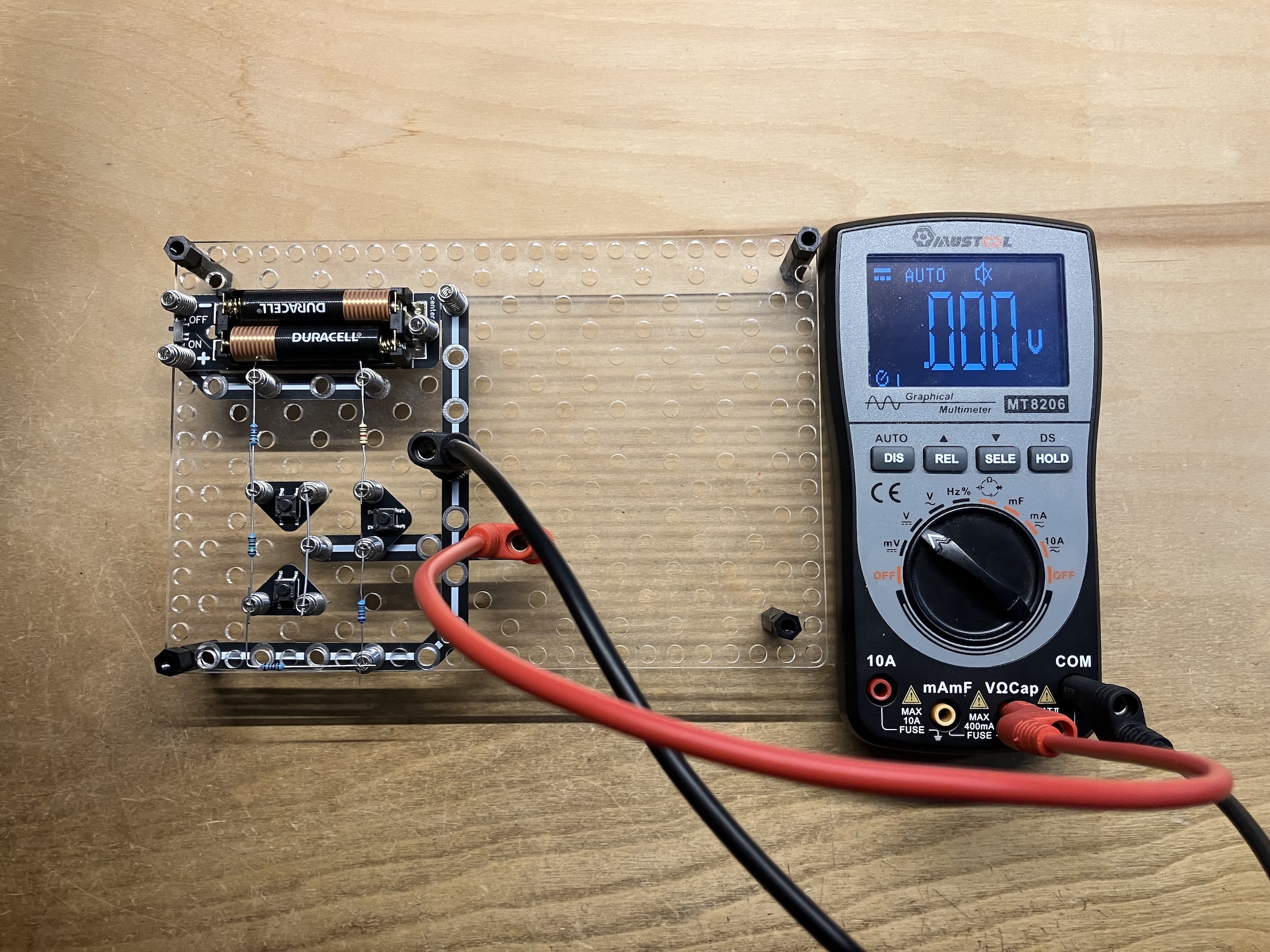
To address the shortcomings of standard ladders, a new configuration has been proposed that manipulates both the "upper" and "lower" portions of the voltage divider simultaneously. By utilizing five resistors for three switches, this circuit achieves a much more uniform distribution of voltage levels.
Comparative Data Analysis
The technical superiority of the novel resistive solution is evident when comparing noise margins and memory footprints.
- Standard Ladder: 59mV noise margin; 162 bytes of flash memory for decoding.
- Novel Resistive Solution: 124mV noise margin; 94 bytes of flash memory for decoding.
The 124mV margin represents a more than 100% improvement in reliability. Furthermore, the reduction in flash memory usage is achieved by aligning the switch voltages with the Most Significant Bits (MSBs) of the ADC output. In a 10-bit ADC system, shifting the value seven bits to the right isolates the three MSBs, which can then be passed through a simple 8-byte lookup table to identify the button state. This eliminates the need for complex, memory-heavy "IF-ELSE" logic trees.

Scaling to Six Inputs
For a six-switch handheld device, this system can be duplicated across two GPIO pins. By sharing certain resistor networks between the two pins, the total component count remains low while maintaining high reliability. This configuration allows for the detection of single button presses and specific dual-button combinations, which is essential for modern user interfaces.
The Diode Ladder: A Binary-Weighted Alternative
For applications where flash memory is at an absolute premium, the "Diode Ladder" offers an even more direct decoding path. This circuit uses the forward voltage drop ($V_f$) of different types of diodes to create a binary-weighted output.
Physics of the Diode Ladder
By using a combination of Schottky diodes (approx. 0.37V drop) and Silicon diodes (approx. 0.7V drop), the circuit creates voltage steps that correspond directly to binary bits. In this scenario, the 3 MSBs of the ADC value directly represent the state of the three switches, potentially removing the need for a lookup table entirely.

Environmental Constraints
Despite its elegance, the diode ladder is sensitive to thermal fluctuations. Diodes typically exhibit a temperature coefficient of -2mV/°C. In extreme environments, a temperature swing of 30°C could shift the voltage by 60mV, potentially causing decoding errors. To mitigate this, engineers suggest incorporating a Negative Temperature Coefficient (NTC) resistor into the network to provide thermal compensation, though this adds complexity back into the hardware.
Broader Implications for Industrial and Maker Communities
The refinement of input multiplexing techniques has significant implications for both mass-market electronics and the "Maker" movement.
Cost and Sustainability
In high-volume manufacturing, the removal of a single IC (like an I2C expander) can save cents per unit. When scaled to millions of devices, this results in hundreds of thousands of dollars in savings. Additionally, reducing the component count aligns with "Green Electronics" initiatives by minimizing the amount of silicon and heavy metals used in consumer products.

Democratization of Hardware Design
For the hobbyist community, these techniques lower the barrier to entry for creating sophisticated devices. Using a $0.50 ATtiny chip instead of a $4.00 ATmega chip allows for the creation of affordable, "disposable" electronics, such as smart badges, simple handheld games, and specialized industrial controllers.
Conclusion
The shift toward smarter, more efficient input multiplexing represents a maturation of microcontroller circuit design. While the industry initially moved toward complex serial protocols to solve pin scarcity, the return to optimized analog solutions proves that clever engineering can often outperform brute-force silicon. By leveraging the inherent capabilities of the ADC and understanding the mathematical properties of resistor networks, designers can squeeze professional-grade functionality out of the most humble components. As the "Internet of Things" (IoT) continues to push for smaller, cheaper sensors and interfaces, these minimal-resource strategies will likely become foundational knowledge for the next generation of embedded systems engineers.