Researchers at the Chalmers University of Technology in Sweden have pioneered a transformative method to enhance the performance of superconducting materials, potentially overcoming the two most significant barriers to their widespread commercial adoption: extreme cooling requirements and sensitivity to magnetic fields. By shifting the focus from the internal chemical composition of the superconductor to the physical architecture of the surface upon which it is grown, the team has demonstrated that nanoscale "sculpting" of a substrate can stabilize superconductivity at higher temperatures and under intense magnetic stress. This development, detailed in the journal Nature Communications, marks a paradigm shift in condensed matter physics and offers a new blueprint for the development of next-generation electronics, quantum computers, and high-efficiency energy grids.
The global urgency for such a breakthrough is underscored by the staggering energy demands of the modern digital age. Current estimates suggest that information and communications technology (ICT) networks, data centers, and digital devices account for between 6 and 12 percent of the world’s total electricity consumption. As artificial intelligence and cloud computing continue to expand, this figure is projected to rise sharply. Traditional silicon-based electronics dissipate a significant portion of their energy as heat due to electrical resistance. Superconductors, which can transport electricity with zero energy loss, offer a theoretical solution to this inefficiency. However, the technical difficulty of maintaining the superconducting state outside of a laboratory setting has, until now, relegated the technology to niche applications like MRI machines and particle accelerators.
The Fundamental Challenge of Superconductivity
Superconductivity was first discovered in 1911 by Heike Kamerlingh Onnes, who observed that mercury lost all electrical resistance when cooled to 4.2 Kelvin (minus 268.95 degrees Celsius). For decades, the phenomenon was thought to be restricted to temperatures near absolute zero, requiring expensive and complex liquid helium cooling systems. The field was revolutionized in 1986 with the discovery of "high-temperature" superconductors—specifically cuprates, which are copper-oxide-based materials. These materials can achieve superconductivity at temperatures above the boiling point of liquid nitrogen (77 Kelvin or minus 196 degrees Celsius), making them significantly more practical, though still far from "room temperature."
Despite the higher thermal threshold of cuprates, they remain notoriously difficult to engineer. Their superconducting properties are highly sensitive to their crystalline structure and the environment in which they are placed. Furthermore, the presence of strong magnetic fields typically disrupts the "Cooper pairs"—the pairs of electrons that move through a superconductor without resistance—causing the material to revert to a resistive state. In many practical applications, such as in the magnets of a fusion reactor or the high-speed processors of a quantum computer, the presence of magnetic fields is unavoidable, creating a catch-22 for engineers.
A Departure from Chemical Manipulation
For decades, the primary strategy for improving superconductors has been chemical doping—the process of introducing specific impurities into the material’s crystal lattice to alter its electronic properties. While this has led to the discovery of various superconducting families, the chemical approach has reached a plateau of diminishing returns. The Chalmers University team, led by Floriana Lombardi, Professor of Quantum Device Physics, decided to abandon the search for new chemical recipes in favor of "interfacial engineering."
The researchers focused on ultrathin films of Yttrium Barium Copper Oxide (YBCO), a well-known cuprate. These films are only a few nanometers thick—roughly one ten-thousandth the width of a human hair. At this scale, the material is highly influenced by the substrate, the underlying foundation on which the superconducting layer is grown. Traditionally, substrates are chosen for their flatness and lattice compatibility, but the Chalmers team theorized that a more active, engineered surface could "template" the superconductor into a more robust state.
"By sculpting the surface that the superconductor rests on, we were able to induce superconductivity at significantly higher temperatures than previously possible," explained Professor Lombardi. "We also found that the material remained superconducting even when exposed to strong magnetic fields."
The Engineering Process: Ridges and Valleys at the Nanoscale
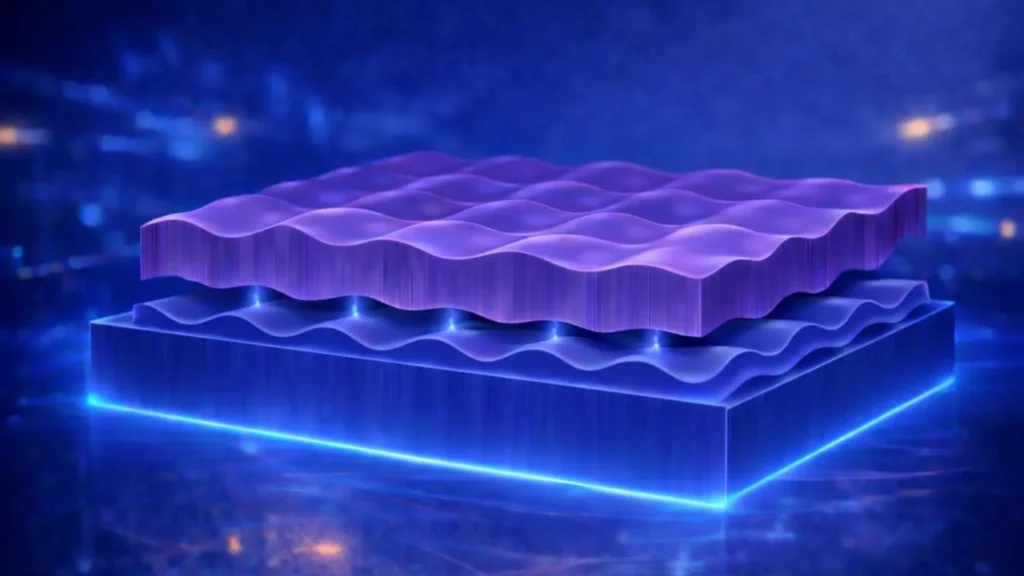
The breakthrough was achieved through a meticulous fabrication process involving high-temperature vacuum treatment of the substrate. Before the YBCO layer was deposited, the team treated the substrate to create a series of nanoscale "ridges and valleys." This "nanofaceted" surface acted as a physical guide for the atoms of the superconducting film as they settled during the growth process.
As the YBCO atoms aligned themselves with the microscopic features of the substrate, the electronic environment at the interface—the thin region where the two materials meet—was fundamentally altered. The researchers observed that the electrons began to exhibit a "preferential direction," a phenomenon that helped stabilize the superconducting state against thermal fluctuations and magnetic interference.
Eric Wahlberg, a researcher at the RISE Research Institutes of Sweden and a key contributor to the study, noted the precision required for this success. "Because the atoms in the substrate are arranged in a specific pattern, they can ‘guide’ how the atoms in the superconducting layer settle. By changing the surface design of the substrate, we were able to influence the superconducting properties and ensure they were preserved."
Data and Performance Metrics
The experimental results provided clear evidence of the method’s efficacy. In standard configurations, ultrathin YBCO films often see a degradation in their critical temperature (Tc)—the point at which they become superconducting—compared to their "bulk" or thicker counterparts. However, the films grown on nanofaceted substrates maintained higher Tc values and showed remarkable resilience to external magnetic fields.
In high-field testing, the engineered films demonstrated a significantly higher "upper critical field"—the maximum magnetic field strength a material can withstand before losing its superconductivity. This suggests that devices built using this technique could operate in environments with electromagnetic interference that would render traditional superconductors useless. Furthermore, the ability to maintain superconductivity in thinner layers is crucial for the miniaturization of electronic components, a prerequisite for integrating superconductors into modern microchips.
Broader Implications for Quantum Computing and Energy
The implications of this research extend far beyond the laboratory. In the realm of quantum computing, superconducting circuits are one of the leading candidates for creating stable qubits. However, these systems are currently hampered by "decoherence," where the quantum state is lost due to environmental noise, including heat and magnetic fluctuations. By providing a more stable superconducting foundation, the Chalmers method could lead to qubits that are less prone to errors and require less aggressive cooling.
In the energy sector, the potential for high-field-resistant superconductors could revolutionize power transmission and storage. Current electrical grids lose an estimated 5 to 10 percent of their energy during transmission due to the resistance of copper and aluminum wires. While superconducting cables exist, their need for constant cooling makes them prohibitively expensive for long-distance use. If substrate engineering can push operating temperatures closer to ambient levels, the dream of a zero-loss global power grid becomes economically viable.
Additionally, the development is significant for the future of clean energy through nuclear fusion. Fusion reactors, such as the ITER project, rely on massive superconducting magnets to confine plasma at temperatures hotter than the sun. These magnets must operate in intense magnetic fields. The ability to "sculpt" more resilient superconductors could lead to smaller, more efficient, and more cost-effective fusion power plants.
A Collaborative Scientific Effort
The study was the result of an extensive international collaboration, highlighting the global interest in high-temperature superconductivity. Researchers from the RISE Research Institutes of Sweden, Uppsala University, and several prestigious institutions in Italy, India, France, and Germany contributed to the findings. The work utilized the Myfab Chalmers cleanroom facility, one of the most advanced nanofabrication labs in Europe.
The project received substantial backing from major funding bodies, including the Swedish Research Council, the Knut and Alice Wallenberg Foundation, and the European Union through an EIC Pathfinder grant. This level of investment reflects the strategic importance of superconductivity in the race for technological sovereignty and sustainable development.
Future Outlook: Toward Room-Temperature Superconductivity
While the Chalmers team has not yet achieved room-temperature superconductivity, their work provides a new roadmap for reaching that "holy grail" of physics. By proving that the physical geometry of the substrate is as important as the chemical makeup of the material, they have opened a new dimension of research.
The next steps for the team involve testing different substrate patterns and exploring whether this technique can be applied to other families of superconducting materials beyond cuprates. There is also the challenge of scaling this nanoscale sculpting process for industrial manufacturing. If the "ridges and valleys" can be produced reliably on a large scale, the transition from silicon-based electronics to superconducting systems could happen sooner than previously anticipated.
"This shows that very small changes at the nanoscale can have decisive effects," Lombardi concluded. "We are now showing how superconductivity can be enhanced by sculpting the substrate, which may even unlock the full potential of superconductivity in future electronics."
As the world grapples with the dual challenges of increasing computational power and reducing carbon footprints, the work coming out of Chalmers University offers a rare glimpse into a future where electronics are not only faster and more powerful but also fundamentally more sustainable. The era of "engineered superconductivity" may have just begun.