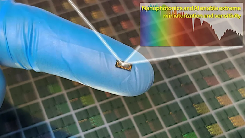
For years, analyzing the chemical makeup of materials has required large and costly laboratory instruments known as spectrometers. These indispensable systems are used in everything from disease diagnosis and food inspection to pollution monitoring and industrial quality control. Traditional spectrometers work by splitting light into its component colors using prisms or gratings, then measuring the intensity of each wavelength. This process, however, necessitates light to travel across a relatively long distance to achieve sufficient spectral resolution, inherently making the instruments bulky, mechanically complex, and exceedingly difficult to miniaturize. The physical constraints have historically limited their deployment, confining advanced spectral analysis primarily to specialized laboratories and high-cost industrial settings. This paradigm is now poised for a dramatic shift, thanks to groundbreaking research from the University of California Davis (UC Davis).
Researchers at UC Davis have engineered a dramatically smaller and more versatile alternative, pushing the boundaries of what is possible in analytical instrumentation. Published in the prestigious journal Advanced Photonics, the team describes a novel spectrometer-on-a-chip so incredibly tiny it approaches the physical dimensions of a single grain of sand. This innovation entirely sidesteps the conventional reliance on large optical components to physically separate light. Instead, the new system harnesses the power of artificial intelligence (AI) and a small array of specially engineered silicon sensors to computationally reconstruct the full light spectrum, marking a significant departure from centuries-old optical principles.
The Historical Challenge of Miniaturization in Spectroscopy
The quest for miniaturized spectrometers has been a long-standing challenge in analytical science. Early spectrometers, dating back to the 19th century with the work of Bunsen and Kirchhoff, were pioneering but rudimentary. Over the past century, advancements in optics, detectors, and data processing have made them incredibly powerful. However, the fundamental principle of dispersing light – whether through prisms, gratings, or interferometers – has remained largely unchanged. These methods demand a certain optical path length to resolve distinct wavelengths, meaning that even with micro-optics, the practical limit for miniaturization has been in the cubic centimeter range, still far too large for true on-chip integration or ubiquitous deployment.
The limitations of traditional bulk spectrometers are multifaceted. Their size makes them unsuitable for integration into portable devices, wearable technology, or remote sensing platforms where space and weight are critical. Their cost, often ranging from tens of thousands to hundreds of thousands of dollars, restricts accessibility. Furthermore, the delicate optical components are susceptible to vibration, temperature fluctuations, and contamination, requiring controlled laboratory environments and frequent calibration. These factors have created a significant barrier to democratizing advanced chemical analysis.
Replacing Bulky Optics With AI: A Paradigm Shift
The core of the UC Davis innovation lies in its audacious abandonment of the standard method of spreading light into a rainbow. Led by Professor Jian-Guo Liu, an expert in integrated photonics and AI, the team’s chip relies instead on an array of 16 unique silicon detectors. Each detector is meticulously designed to react slightly differently to incoming light, exhibiting a distinct spectral response profile. Rather than attempting to isolate individual colors directly, these detectors collect a series of encoded signals, each containing fragmented yet crucial spectral information.
"Imagine a choir where each singer has a slightly different voice and sings a unique part of the melody," explains Professor Liu. "Individually, you might not hear the whole song, but when you combine all their voices, a trained ear can reconstruct the complete piece. Our detectors work similarly, each providing a unique ‘taste’ of the light’s composition."
This analogy helps to conceptualize the system’s operation. Individually, each detector only captures a partial and often ambiguous picture of the incoming light’s spectrum. Together, however, they generate a complex matrix of data—a unique "fingerprint" for each incident light spectrum. This raw, encoded information is then fed into the second key component: a fully connected neural network.
The neural network, a form of artificial intelligence, is the brain of the spectrometer. It was rigorously trained on thousands of examples, learning the intricate and often non-linear relationship between the noisy, highly encoded signals from the 16 detectors and the actual, full spectrum of light. This process effectively solves what researchers call an "inverse problem." In traditional spectroscopy, one measures the spectrum directly to infer the sample’s composition (a forward problem). Here, the system starts with complex, indirect measurements and uses AI to work backward, reproducing the spectral data with remarkable accuracy, achieving a resolution of approximately 8 nanometers (nm) across a broad spectral range without a single bulky optical component. This resolution is comparable to many entry-level laboratory spectrometers, a staggering achievement for a device of this size.
Expanding Silicon’s Reach: The Near-Infrared Breakthrough
A major technological breakthrough critical to the chip’s versatility came from addressing one of silicon’s inherent limitations. Standard silicon photodiodes excel at detecting visible light but historically struggle to capture near-infrared (NIR) light, typically wavelengths up to 1100 nm. This limitation has been a significant hurdle for many potential applications, as NIR light is of paramount importance in fields such as biomedical imaging, industrial process control, and environmental monitoring. For instance, NIR light can penetrate deeper into human tissue than visible light, making it invaluable for non-invasive diagnostics, blood oxygenation measurements, and even early cancer detection.
To overcome this, the UC Davis team modified the surface of standard silicon photodiodes with specialized photon-trapping surface textures (PTSTs). These intricately engineered nanostructures fundamentally alter how light behaves within the thin silicon layer. Instead of allowing NIR photons to pass straight through the material—a common occurrence due to silicon’s relatively weak absorption in this range—the textured surface scatters the light repeatedly, trapping it within the silicon. This enhanced interaction dramatically increases the likelihood that the silicon will absorb the NIR photons, generating an electrical signal.
"The PTSTs act like a labyrinth for light," explains Dr. Sarah Chen, a co-author on the study, "forcing the photons to bounce around inside the silicon until they are finally absorbed. This simple yet elegant solution effectively extends silicon’s sensitivity far into the near-infrared, unlocking a vast array of new applications for our chip." As a result of this ingenious engineering, the chip becomes sensitive across a much wider spectral range than conventional silicon sensors, broadening its utility exponentially.
Beyond Static Spectra: Capturing Ultrafast Light Interactions
The new architecture offers more than just the ability to detect and reconstruct static color spectra. The UC Davis chip also incorporates high-speed sensors capable of measuring photon lifetime with extremely high temporal precision. This advanced capability allows the device to detect ultrafast interactions between light and matter—phenomena that occur on picosecond or even femtosecond timescales. Traditional, bulk spectrometers, with their inherent physical limitations, often miss these dynamic, transient interactions entirely.
The ability to measure photon lifetime, also known as time-resolved spectroscopy, provides a deeper layer of information about a material’s properties. For example, it can reveal details about molecular structure, energy transfer processes, and even the presence of specific biomarkers. "This capability is a game-changer," states Professor Liu. "It means we’re not just seeing what colors are present, but how light is interacting with matter at an incredibly fundamental level. This could open the door to advanced forms of sensing and imaging that previously required far larger, more complex, and prohibitively expensive systems, often involving pulsed lasers and specialized detectors."
A Tiny Footprint With Big Potential: Implications and Applications
The completed system is a marvel of miniaturization, occupying just 0.4 square millimeters. Despite its minuscule size, it maintains high sensitivity and demonstrates strong resistance to electrical noise, a persistent and major challenge for portable, low-cost electronics. Even in electrically noisy environments, the AI-assisted design can preserve clear signal quality, a critical factor for real-world deployment.
By seamlessly combining sophisticated machine learning algorithms with enhanced silicon light detection technology, this innovation could pave the way for a new generation of compact, real-time hyperspectral sensing devices. The implications span numerous sectors:
- Medical Diagnostics: Imagine a wearable device that continuously monitors blood glucose levels non-invasively, or a handheld device for rapid, point-of-care disease diagnosis in remote areas. The ability to detect NIR light and measure photon lifetimes could revolutionize early detection of conditions like skin cancer or cardiovascular disease.
- Food Quality and Safety: Portable spectrometers could allow consumers or inspectors to instantly verify the ripeness of fruit, detect contaminants in food products, or assess nutritional content on the spot, ensuring safer and healthier food supply chains.
- Environmental Monitoring: Miniaturized sensors could be deployed in vast networks to monitor air and water quality, detect pollutants, or identify chemical spills in real-time, providing crucial data for environmental protection and disaster response.
- Industrial Process Control: Industries could integrate these chips directly into manufacturing lines for continuous, real-time quality control of materials, optimizing production and reducing waste.
- Agriculture: Farmers could use drone-mounted or handheld devices to analyze soil composition, plant health, and nutrient deficiencies across vast fields, leading to more efficient resource management and increased yields.
- Defense and Security: Compact chemical threat detection systems could be developed for rapid identification of hazardous substances, enhancing safety for personnel.
Expert Reactions and the Road Ahead
The scientific community has reacted with considerable enthusiasm to the UC Davis breakthrough. Dr. David Miller, a prominent photonics researcher at MIT who was not involved in the study, commented, "This work represents a significant leap forward in integrated photonics. The clever integration of AI with novel silicon engineering to overcome fundamental optical limitations is truly impressive. It addresses a long-standing need for compact, robust, and affordable spectroscopic tools, and I foresee its impact reverberating across many scientific and industrial disciplines."
The development timeline for such a complex technology typically involves several stages. The initial research and proof-of-concept, culminating in the Advanced Photonics publication, represent years of dedicated effort. The next phases will likely focus on further optimization of the chip’s performance, increasing its spectral resolution, and expanding its detection range. Following this, efforts will turn towards robust packaging, mass manufacturability, and rigorous field testing in diverse application scenarios.
While the potential is immense, challenges remain. Scaling production of such highly specialized silicon devices, ensuring consistent performance across millions of units, and developing user-friendly interfaces for complex AI algorithms will require substantial engineering and investment. Regulatory approvals, particularly for medical applications, will also be a lengthy process. However, the fundamental science and engineering hurdles have been largely overcome.
The UC Davis spectrometer-on-a-chip is more than just a smaller instrument; it represents a paradigm shift in how we approach chemical analysis. By replacing bulky optics with intelligent, data-driven computational methods and pushing the limits of silicon photonics, researchers have opened the door to a future where advanced analytical capabilities are not confined to the laboratory but are ubiquitous, integrated into our daily lives, and accessible to anyone, anywhere. This tiny chip has the potential to make a big difference in understanding our world, from the microscopic interactions within our bodies to the vast complexities of our environment.