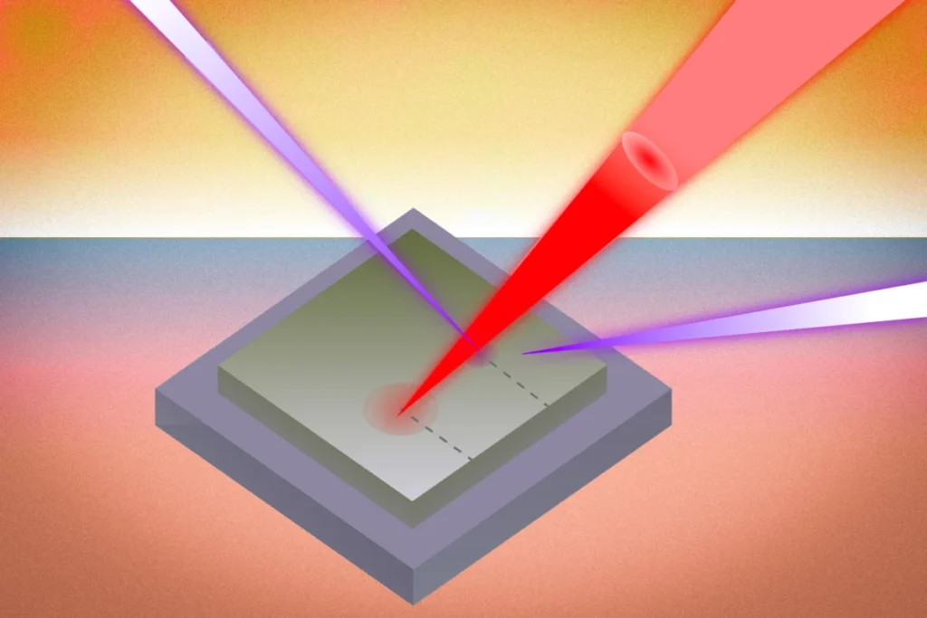
The persistent challenge of thermal management, which causes consumer laptops to throttle and massive data centers to consume gargantuan amounts of electricity for cooling, has met a formidable new adversary in a diagnostic breakthrough from the Massachusetts Institute of Technology. As the semiconductor industry pushes the limits of Moore’s Law, cramming billions of transistors into increasingly compact, multilayered architectures, the inability to accurately track heat dissipation at the microscopic level has become a primary barrier to further innovation. To address this, a multidisciplinary team of MIT researchers has demonstrated a novel imaging technique that utilizes high-intensity X-rays and ultrafast laser pulses to visualize heat movement through complex, multi-layered electronic devices in real-time.
This new methodology, recently detailed in the journal Nature Communications, represents a significant leap forward from traditional thermal measurement techniques. By combining the penetrative power of X-rays with the precision of laser-induced heating, the researchers have successfully quantified how heat traverses internal interfaces—a feat previously thought nearly impossible due to the opaque nature of modern semiconductor "sandwiches." The findings reveal that even microscopic defects, previously dismissed as negligible, can catastrophically impede heat flow, providing a roadmap for engineers to design the high-performance, power-dense electronics required for the next generation of artificial intelligence (AI), wearable technology, and clean energy systems.
The Thermal Wall: A Growing Crisis in Modern Computing
For decades, the trajectory of the electronics industry has been defined by miniaturization. However, as components shrink to the nanometer scale, the density of heat generation increases exponentially. In modern data centers, which power everything from global financial networks to generative AI models, thermal management is no longer just a maintenance concern; it is a fundamental design constraint. High temperatures degrade the performance of silicon chips, reduce the lifespan of hardware, and necessitate massive investments in liquid cooling and HVAC systems.
The core of the problem lies in the "multilayered" nature of modern electronics. A contemporary computer chip is not a single slab of material but a complex stack of semiconductors, insulators, and metallic interconnects. When heat is generated at the transistor level, it must travel through several layers and across numerous interfaces to reach a heat sink. Understanding how heat moves through these buried layers is essential for optimizing performance.
Traditional diagnostic tools, however, have been found wanting. Optical methods like time-domain thermal reflectance (TDTR) are limited by the physics of light; they can only "see" what is happening at or near the surface of a material. Infrared thermography, while useful for macroscopic views, lacks the spatial resolution and frame rate necessary to capture the ultrafast, nanometer-scale movement of heat carriers known as phonons. This lack of visibility has forced engineers to rely on theoretical models that often assume "perfect" material conditions—an assumption that rarely holds true in the high-volume manufacturing of real-world devices.
The MIT Innovation: Ultrafast X-Rays and Laser Pulses
To break through this visibility barrier, the MIT research team, led by Mingda Li, an associate professor of nuclear science and engineering, and Jeehwan Kim, an associate professor of mechanical engineering and materials science and engineering, looked toward the most powerful diagnostic tools available in modern physics.
The team’s approach utilizes a combination of two distinct technologies: ultrafast laser pulses and high-brightness X-rays. In their experimental setup, a laser pulse is used to deliver a precise "kick" of heat to a specific spot on a device. Simultaneously, an X-ray beam—sourced from the Advanced Photon Source at Argonne National Laboratory—is directed at the material. Because X-rays have a much shorter wavelength than visible light, they can penetrate through multiple layers of a device, reaching the buried interfaces where heat often becomes trapped.
The X-rays do not measure temperature directly in the way a thermometer does. Instead, they measure "lattice strain." When a material heats up, its atoms vibrate more vigorously, causing the crystal lattice to expand or distort. By measuring how the X-rays diffract off these atoms, the researchers can calculate the exact degree of strain and, by extension, the precise temperature and heat flow at specific points within the multilayered structure.
"Over the last few years, researchers have developed what is basically the brightest X-ray source in the world," explains Thanh Nguyen, a PhD graduate and co-lead author of the study. "That allows you to focus an X-ray beam and get incredibly fine spatial resolution. You can also use a laser to heat the sample while the X-ray scans and shows how the heat dissipates across space in real-time."
Case Study: The Hidden Impact of Micron-Scale Defects
To test the efficacy of their new tool, the researchers applied it to a promising material stack: gallium nitride (GaN) grown on a silicon substrate. Gallium nitride is a "wide-bandgap" semiconductor that is increasingly favored over traditional silicon for high-power applications, such as the inverters used in electric vehicles and the power supplies for AI server racks. While GaN is theoretically an excellent thermal conductor, its real-world performance has often lagged behind expectations.
Using their X-ray technique, the MIT team discovered why. They focused on a common manufacturing flaw known as a "wrinkle defect"—a microscopic ripple in the material caused by the mismatch in atomic spacing between the GaN and the silicon.
The results were startling. The researchers found that a single micron-scale wrinkle caused a fourfold reduction in the material’s ability to transfer heat at that specific spot. Furthermore, the defect caused the heat to spread anisotropically, meaning it moved much more easily in one direction than the other. This uneven distribution creates "hotspots" that can lead to localized failures, even if the average temperature of the chip remains within safe limits.
"When people model heat dissipation, they model perfect crystals without defects," says Professor Mingda Li. "But these types of large wrinkle defects are very common in 2D materials. People never even knew how much heat is blocked by these wrinkles. Those are things we can now directly observe with this technique."
Industry Response and Economic Implications
The implications of this research have already resonated within the semiconductor industry. A leading semiconductor industry consortium has reportedly already reached out to the MIT team to explore how this measurement technique can be integrated into the research and development cycles for next-generation chips.
The ability to diagnose thermal bottlenecks at the micro-scale offers a massive competitive advantage. For companies like NVIDIA, Intel, and TSMC, the goal is to pack more processing power into smaller footprints. If engineers can identify exactly where heat is getting stuck—whether it is at a specific material interface or due to a particular manufacturing defect—they can adjust their fabrication processes to eliminate those barriers.
From an economic perspective, improving thermal efficiency is a matter of global energy security. Data centers currently account for approximately 1% to 2% of global electricity consumption, a figure expected to rise sharply with the proliferation of AI. A significant portion of that energy is wasted as heat or used to power cooling fans and chillers. By designing chips that naturally dissipate heat more effectively, the industry can reduce the carbon footprint of the digital economy.
Future Applications: From Wearables to Clean Energy
While the current study focused on GaN-on-silicon, the researchers emphasize that the technique is material-agnostic. It can be applied to a wide range of emerging technologies:
- Flexible Electronics and Wearables: Devices that must bend and stretch often use 2D materials that are prone to the very types of wrinkle defects identified in the MIT study. Ensuring these devices don’t overheat while in contact with human skin is a critical safety and comfort requirement.
- Quantum Computing: Quantum processors operate at temperatures near absolute zero. Even the slightest heat leakage can decohere qubits. This X-ray technique could help researchers design more effective thermal shielding for quantum systems.
- Clean Energy Systems: Power electronics in solar inverters and electric vehicle chargers handle high voltages and currents. Improving heat flow in these systems allows for smaller, lighter, and more efficient energy conversion hardware.
Conclusion and Research Outlook
The MIT team’s work, supported by the U.S. Department of Energy and the National Science Foundation, marks a turning point in the field of thermal metrology. By moving beyond surface-level observations and into the deep, multilayered heart of electronic devices, they have provided the industry with a "microscope" for heat that was previously missing.
"Chip developers need devices that can handle heat," says Professor Li. "I think overheating has become the real bottleneck in device performance. This approach is a step toward understanding exactly what causes failure, in order to avoid local hotspots and design better devices."
As the semiconductor industry enters the era of "3D integration"—where chips are stacked vertically to increase density—the complexity of heat flow will only grow. The ability to use ultrafast X-rays to see through these stacks and identify thermal roadblocks ensures that the next generation of computing power will not be held back by the very heat it generates. The MIT researchers plan to continue refining the technique, aiming for even higher spatial and temporal resolutions to track the movement of individual phonons, the fundamental particles of heat.