The persistent challenge of overheating, a familiar adversary to laptop users, presents an even more critical bottleneck for the global network of computer servers and vast data centers. As semiconductor technology continues its relentless march towards ever more compact and powerful chips, the ability to effectively manage and dissipate heat has become the paramount hurdle limiting performance, reliability, and energy efficiency. Understanding the intricate pathways of heat transfer at the micro- and nanoscale within these complex, multilayered devices is not merely an academic pursuit but an essential requirement for sustained innovation in the electronics industry. Traditional methods, however, have largely fallen short in providing the granular, layer-specific insights needed for modern chip architectures.
Now, researchers at the Massachusetts Institute of Technology (MIT) have unveiled a groundbreaking technique that promises to fundamentally transform how heat flow is studied within these critical components. Demonstrating a novel approach published in Nature Communications, the team has successfully combined the penetrating power of X-rays with the precise energy delivery of laser pulses to meticulously track heat movement through multilayered materials. This innovative methodology offers an unprecedented level of precision, enabling scientists and engineers to peer into the hidden thermal dynamics of devices that power our digital world, from artificial intelligence (AI) applications to cutting-edge wearables and vital clean energy systems.
The Pervasive Challenge of Thermal Management in Modern Electronics
For decades, the semiconductor industry has largely followed Moore’s Law, doubling the number of transistors on an integrated circuit approximately every two years. This exponential increase in transistor density, coupled with rising clock speeds, has been the primary driver of the computational power that defines the modern technological landscape. However, this progress has come with a significant thermal cost. As more transistors are packed into smaller areas, operating at higher frequencies, the power density—and consequently, the heat generated—within these chips escalates dramatically.
The repercussions of this escalating heat generation are manifold and far-reaching. At the consumer level, it manifests as laptops growing uncomfortably warm or smartphones throttling performance to prevent damage. In the enterprise sector, the implications are far more severe. Data centers, the colossal engines of the internet and cloud computing, consume staggering amounts of energy, a substantial portion of which is dedicated not to computation itself, but to cooling the servers. Estimates suggest that cooling can account for 30% to 50% of a data center’s total energy consumption. Globally, data centers are projected to consume around 1-2% of the world’s electricity, a figure that is expected to rise as demand for digital services continues to surge. In 2023, the global data center market was valued at hundreds of billions of dollars, with thermal management solutions alone representing a multi-billion-dollar segment. The economic and environmental imperative to improve thermal efficiency is thus undeniable.
The increasing heat flux density in modern processors rivals that of a nuclear reactor or a hot plate, pushing the boundaries of conventional cooling solutions. Beyond immediate performance degradation, sustained high temperatures accelerate material degradation, reduce component lifespan, and increase the risk of catastrophic device failure. This phenomenon, often referred to as the "thermal wall," has emerged as a significant impediment to further advancements in chip design, forcing engineers to make difficult trade-offs between performance, power consumption, and physical size.
Limitations of Conventional Heat Flow Measurement
Addressing the thermal wall requires a detailed understanding of how heat propagates, dissipates, and accumulates within a device. However, traditional techniques for measuring heat flow have inherent limitations, particularly when confronted with the complex, multilayered architectures characteristic of modern electronics.
One widely used optical method is Time Domain Thermal Reflectance (TDTR). While effective for studying heat at the microscopic level, TDTR primarily probes the surface of a material. As MIT Associate Professor Jeehwan Kim explains, "Because that technique uses optics, it doesn’t allow you to study different layers. Real devices have five or more layers. It also only provides an overall signal, and that makes it hard to see thermal transport happening in layers buried under the surface." This limitation renders TDTR less effective for diagnosing issues in the intricate, stacked designs prevalent in advanced processors, memory chips, and novel flexible electronics, where interfaces between different materials play a crucial role in thermal transport.
Other approaches, such as infrared cameras, offer macroscopic views of temperature distribution but lack the spatial and temporal resolution required to capture the rapid, tiny changes occurring at the micro- or nanometer scale. These techniques provide an aggregated, averaged picture, obscuring the localized "hotspots" and microscopic defects that are often the root cause of thermal performance degradation. The inability to precisely pinpoint these issues has left chip developers largely operating in the dark when it comes to optimizing thermal design at the foundational material level.
MIT’s Revolutionary X-ray and Laser-Pulse Methodology
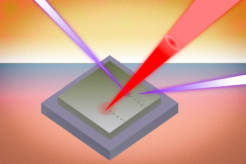
Recognizing this critical gap, the MIT research team set out to develop a technique capable of measuring heat transfer at the nanoscale within complex multilayer systems. Their solution harnesses the power of an emerging analytical method that combines ultrafast X-rays with laser-powered electron pulses. The core innovation lies in leveraging the unique properties of these energy sources.
As co-lead author Thanh Nguyen, PhD ’24, elaborated, "Over the last few years, researchers have developed what is basically the brightest X-ray source in the world. That allows you to focus an X-ray beam and get incredibly fine spatial resolution. You can also use a laser to heat the sample while the X-ray scans and shows how the heat dissipates across space in real-time."
The technique works by first applying a precisely timed laser pulse to a specific point on the material, introducing a localized burst of heat. Simultaneously, ultrafast X-rays are directed at the sample. Unlike optical methods, X-rays possess the energy and penetrating power to pass through multiple layers of a material, interacting with the atomic lattice within. As heat propagates through the material, it causes minute changes in the atomic structure and strain. The X-rays detect these changes through diffraction patterns, providing a real-time, three-dimensional map of how heat moves through and across different layers and interfaces.
Co-lead author and MIT postdoc Chuliang Fu highlighted the advantage: "Using previous measurement techniques, in real devices, you couldn’t resolve what happens on one layer versus another, so you’d just measure the average. X-rays can clearly show how heat propagates across the interface through their diffraction." This combination of deep penetration, high spatial resolution, and ultrafast temporal resolution allows the researchers to track the dynamic process of heat dissipation with unprecedented clarity. The measurements from the laser-powered electron pulse (capturing atomic-level strain) and the X-rays (penetrating multiple layers) are then combined to construct a comprehensive view of the material’s thermal behavior.
Unveiling Hidden Flaws: The Gallium Nitride Case Study
To validate their new technique, the MIT team applied it to a test device composed of gallium nitride (GaN) layered on top of silicon. Gallium nitride is a wide-bandgap semiconductor material that has garnered significant interest for its potential in high-power, high-frequency applications, including next-generation transistors and flexible electronics, largely due to its superior electron mobility and breakdown voltage compared to traditional silicon. However, the thermal performance of GaN devices has historically been hampered by microscopic defects that often arise during the fabrication process.
The results of the MIT team’s measurements were striking and revealed a level of detail previously unattainable. Their technique allowed them to quantify the exact impact of a single micron-scale defect—a wrinkle—on the device’s thermal properties. They discovered a surprising fourfold reduction in the material’s ability to transfer heat at that precise spot. Furthermore, the analysis revealed that this defect caused heat to spread unevenly, exhibiting anisotropic behavior, meaning it moved more easily in one direction than in another. Beyond this specific defect, the researchers observed an overall 25% drop in heat dissipation across the materials, indicating a more significant disruption to thermal flow than conventional models, which often assume perfect crystals, had anticipated.
As Associate Professor Mingda Li, an associate professor of nuclear science and engineering at MIT and co-corresponding author on the paper, explained, "When people model heat dissipation, they model perfect crystals without defects. But these types of large wrinkle defects are very common in 2D materials. People never even knew how much heat is blocked by these wrinkles. Those are things we can now directly observe with this technique." This finding is particularly significant because it underscores the limitations of idealized theoretical models and highlights the critical need for experimental validation that accounts for real-world manufacturing imperfections.
The team behind this breakthrough includes co-lead authors Thanh Nguyen PhD ’24 and MIT postdoc Chuliang Fu, alongside PhD candidate Mouyang Cheng; Abhijatmedhi Chotrattanapituk ’21, SM ’26; Denisse Córdova Carrizales SM ’26; Eunbi Rha SM ’26; Tyra Espedal ’26; Buxuan Li PhD ’24; Shivam Kajale SM ’23, PhD ’26; Tongtong Liu PhD ’23; Kuan Qiao PhD ’22; University of Texas at Austin Assistant Professor Zhantao Chen SM ’18, PhD ’22; Argonne National Laboratory researchers Kumar Neeraj, Donald Walko, and Haidan Wen; MIT Principal Research Scientist Svetlana Boriskina; MIT Associate Professor Deblina Sarkar; and co-corresponding author and MIT Associate Professor Jeehwan Kim. Their collaborative efforts across various disciplines underscore the complexity and interdisciplinary nature of modern scientific discovery.
Broader Implications for Technology and Industry
The implications of MIT’s new thermal measurement technique are profound and extend across a multitude of technological sectors. By providing unprecedented insight into the thermal performance of materials and devices, this approach is poised to accelerate innovation and overcome long-standing design challenges.
AI and High-Performance Computing (HPC): The insatiable demand for computational power, particularly in the fields of artificial intelligence, machine learning, and data analytics, relies heavily on advanced GPUs and specialized AI accelerators. These chips generate immense heat. Better thermal management enabled by this new technique can allow for even higher transistor densities, faster clock speeds, and more aggressive chip architectures, ultimately leading to more powerful and efficient AI systems capable of handling larger datasets and more complex models. This could unlock new frontiers in scientific discovery, medical diagnostics, and autonomous systems.
Wearables and Internet of Things (IoT): For compact devices like smartwatches, fitness trackers, and a vast array of IoT sensors, miniaturization and energy efficiency are paramount. The ability to precisely manage heat within these confined spaces means devices can be made smaller, lighter, and more comfortable, while also extending battery life and improving reliability. This is crucial for the continued expansion of ubiquitous computing.
Clean Energy Systems: Power electronics are fundamental to modern clean energy infrastructure, including electric vehicles (EVs), solar inverters, and wind turbine converters. These systems often operate under high current and voltage conditions, generating significant heat. Optimizing the thermal design of components like power transistors and diodes using the MIT technique can lead to more efficient energy conversion, reduced power losses, and enhanced durability for critical green technologies, accelerating the transition to a sustainable future.
Semiconductor Manufacturing and Design: The direct observation of how defects impact thermal flow provides invaluable feedback for semiconductor manufacturers. This insight can guide improvements in material growth processes, fabrication techniques, and quality control measures, leading to the production of more thermally robust and reliable chips. As Professor Li noted, "Chip developers need devices that can handle heat. I think overheating has become the real bottleneck in device performance." This technique offers a direct pathway to overcoming this bottleneck by enabling targeted design improvements.
The significance of this breakthrough has not gone unnoticed by industry. Professor Li revealed that a "leading semiconductor industry consortium has already reached out to collaborate on applying the measurement technique to study different types of chips." This immediate interest from a major industry player underscores the pressing need for such diagnostic capabilities and suggests a potential for rapid adoption and integration into mainstream R&D.
Economic and Environmental Impact
The broader economic and environmental implications are substantial. Reducing the energy consumption associated with cooling data centers, for instance, could translate into billions of dollars in annual savings globally, while simultaneously cutting down on greenhouse gas emissions. Improved chip reliability means longer device lifespans, reducing electronic waste and the need for frequent replacements. For the semiconductor industry, faster innovation cycles and the ability to push performance boundaries without being limited by thermal constraints could lead to significant competitive advantages and new market opportunities.
Furthermore, this method’s capability to study fundamental thermal transport mechanisms, such as the behavior of "heat carriers," opens doors for deeper scientific understanding. This foundational knowledge is crucial for developing entirely new materials with inherently superior thermal properties, moving beyond incremental improvements in existing designs.
Looking Ahead: The Path to Cooler, More Powerful Electronics
The MIT researchers are confident that their approach will serve as a foundational tool for the next generation of electronic design. "We can now pass a current and shine an X-ray on a device and see how the heat dissipates at a very small scale," Professor Kim stated, emphasizing, "That’s something the industry has been longing for."
This innovative diagnostic capability marks a significant departure from previous methodologies that provided only averaged thermal signals. By offering direct, high-resolution experimental measurements of heat flow within complex geometries and across multiple material layers, the technique empowers engineers to make informed design decisions. "This will enable better thermal design of electronic systems," Kim concluded. "Even with the same type of materials, the geometry and how the materials are laid out is quite complicated, so it will show us how those differences impact thermal flow by providing direct experimental measurements."
Supported by funding from the U.S. Department of Energy, the U.S. National Science Foundation, and the MIT School of Engineering Distinguished Energy Efficiency Fellowship, this research represents a critical step towards overcoming the thermal limitations that have long constrained the evolution of electronics. As devices become increasingly power-dense and miniaturized, the ability to precisely diagnose and mitigate heat-related issues will be paramount. The MIT team’s breakthrough offers a clear path forward, paving the way for a future where electronic devices are not only more powerful and efficient but also inherently cooler and more reliable.