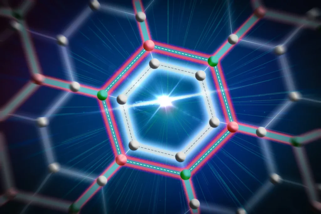
In a development that could fundamentally reshape the trajectory of quantum hardware development, researchers at the Massachusetts Institute of Technology (MIT) have successfully engineered a new process to produce monolayer superconductors at a wafer-scale while maintaining their stability in ambient conditions. The research, published today in the journal Nature, details a sophisticated "growth-under-graphene" technique that protects fragile two-dimensional materials from oxidation, solving a decades-old bottleneck in the field of materials science. By integrating these ultrathin materials into superconducting microwave circuits, the team has demonstrated that these films retain high kinetic inductance and robust superconducting properties, paving the way for the radical miniaturization of quantum computers and ultra-sensitive detectors for cosmology.
The Evolution of Two-Dimensional Superconductors
Superconductors are materials capable of conducting electricity with zero energy loss. While they have been the cornerstone of high-performance magnets and medical imaging for decades, their application in quantum computing has traditionally relied on bulk materials or thin films that are relatively thick by atomic standards. The emergence of two-dimensional (2D) superconductors—materials only a few atoms thick—offered a theoretical promise of extreme miniaturization. Among these, niobium diselenide ($NbSe_2$) has stood out due to its unique electronic properties and high kinetic inductance.
Niobium diselenide is a transition metal dichalcogenide (TMD) composed of a single layer of niobium atoms sandwiched between two layers of selenium atoms. Despite its potential, $NbSe_2$ has historically been plagued by extreme atmospheric instability. When exposed to oxygen or moisture, even for a few seconds, the monolayer structure begins to oxidize, destroying its superconducting capabilities. Until now, scientists were forced to rely on "exfoliation"—using adhesive tape to peel small flakes from a larger crystal—which resulted in tiny, irregular samples that could only be studied in vacuum or inert environments. This "Scotch-tape method" is insufficient for industrial-scale manufacturing or the creation of complex integrated circuits.
The Innovation: Growth Under the Graphene Umbrella
The MIT-led team, which included collaborators from New York University, Rice University, Yale University, and South Korea’s Pohang University, devised a counterintuitive solution to the oxidation problem. Rather than growing the superconductor and then attempting to protect it, they flipped the process entirely.
The researchers first deposited a layer of graphene—a single layer of carbon atoms—onto a silicon dioxide substrate. They then introduced the chemical precursors for niobium diselenide. Through a process of carefully tuned chemical vapor deposition, the precursors migrated into the infinitesimal gap between the graphene and the silicon dioxide. Despite the graphene being placed directly on the substrate, the weak Van der Waals forces between the materials leave a gap of less than one nanometer.
"It took a long time for us to understand how the growth could happen underneath the graphene," said co-lead author Xudong Sheldon Zheng, a graduate student in the MIT Department of Electrical Engineering and Computer Science (EECS). "Through collaboration and discussion, we eventually uncovered the mechanism for growing the material at the interface, and this solves a lot of problems and allows us to simplify our fabrication steps."
The graphene layer serves a dual purpose: it acts as a "molecular umbrella," shielding the growing $NbSe_2$ from the atmosphere, and its smooth surface allows the precursors to move freely, resulting in a continuous, uniform monolayer. Using this method, the team successfully generated smooth superconducting films over an inch in diameter—a significant leap from the micrometer-scale flakes produced by previous methods.
Technical Analysis: The Power of Kinetic Inductance
A critical finding of the research is the material’s high kinetic inductance. In the realm of superconducting circuits, inductance is the property that allows a material to store energy in a magnetic field. However, in ultrathin superconductors, "kinetic" inductance arises from the inertia of the superconducting electrons (Cooper pairs) themselves.
Modern superconducting quantum bits (qubits) often require large amounts of inductance to operate correctly and to remain protected from noise. Currently, engineers achieve this by stringing together hundreds of Josephson junctions—complex electronic components—into long arrays. These arrays take up significant "real estate" on a quantum chip, limiting how many qubits can be packed onto a single wafer.
By utilizing monolayer $NbSe_2$, which naturally possesses high kinetic inductance due to its thinness and electronic structure, researchers can replace these bulky arrays with a single, tiny strip of material. This could reduce the footprint of certain circuit elements by orders of magnitude. The MIT team’s tests showed that the material maintained this high kinetic inductance even after being integrated into microwave circuits, proving its viability as a functional component in quantum processors.
Overcoming the Integration Hurdle
Producing the material was only half the battle. Integrating a 1-nanometer-thick film into a circuit with electrodes that are hundreds of nanometers thick presents a massive engineering challenge. Standard fabrication techniques often damage the edges of 2D materials, leading to poor electrical contact.
To solve this, the researchers developed an oxidation-free transfer technique to peel the graphene-$NbSe_2$ heterostructure from its growth substrate. Co-lead author Sameia Zaman, an EECS graduate student, explained the difficulty: "It is challenging to make a good electrical connection between this very thin material and our electrodes. We had to develop a method to etch the side walls of the thin-film superconductor in a vacuum chamber to preserve the smooth edge of the material."
By maintaining a pristine interface between the $NbSe_2$ and the conventional superconducting electrodes, the team achieved reliable electrical connections. This breakthrough ensures that the material can be used in "clean room" environments to create sophisticated, multi-layered quantum devices without losing its unique properties.
Chronology and Research Context
The journey toward this discovery has been years in the making. The research builds upon previous milestones in the study of 2D materials:
- 2004: Graphene is first isolated, sparking global interest in 2D materials.
- 2010s: Discovery of superconductivity in monolayer $NbSe_2$, though samples are unstable and small.
- 2020-2022: MIT researchers begin exploring "interfacial growth" techniques to encapsulate TMDs.
- 2023: The team refines the growth parameters to achieve wafer-scale uniformity.
- 2024 (Present): Publication in Nature demonstrating the first air-stable, wafer-scale, integrated monolayer superconducting circuit.
The study was a massive collaborative effort. Zheng and Zaman were joined by co-lead author Kenan Zhang, a former postdoc in the MIT Research Laboratory of Electronics (RLE). The project was guided by senior corresponding authors William D. Oliver, a professor of physics and director of the Center for Quantum Engineering; Jing Kong, the Jerry McAfee Professor in Engineering at MIT; and Joel I-J. Wang of NYU.
Broader Implications and Future Applications
The ability to mass-produce stable, ultrathin superconductors has implications that extend far beyond the laboratory.
1. Quantum Computing Scalability:
The primary bottleneck for quantum computers today is the physical size and error rate of qubits. By using high-inductance 2D materials, engineers can design more compact circuits, potentially allowing for thousands more qubits on a single chip than current technology permits.
2. Ultrasensitive Detectors:
In the field of cosmology, scientists use superconducting detectors to measure the cosmic microwave background radiation—the "afterglow" of the Big Bang. The high sensitivity and low noise of monolayer $NbSe_2$ could lead to a new generation of detectors capable of peering deeper into the history of the universe.
3. Quantum Communications:
High-kinetic-inductance materials are essential for creating single-photon detectors used in secure quantum communication networks. The MIT process makes these materials more accessible for commercial-scale deployment.
4. Fundamental Physics:
Scientists can now study the "Berezinskii-Kosterlitz-Thouless" (BKT) transition and other exotic states of matter in 2D superconductors with greater precision, as they no longer have to worry about the samples degrading mid-experiment.
Funding and Institutional Support
The ambitious project received support from a diverse array of governmental and private institutions, reflecting the strategic importance of quantum materials. Funding was provided by the U.S. Army Research Office, the National Science Foundation (NSF), the U.S. Department of Energy (DOE), and the Air Force Office of Scientific Research. International support came from the National Research Foundation of Korea and the Schlumberger Foundation. Much of the fabrication and characterization work was performed at MIT.nano, the university’s state-of-the-art facility for nanoscience and nanotechnology.
As the research moves forward, the team aims to integrate these monolayers into even more complex architectures. "We’ve taken a very good step toward exploring both the physics and the application side of this thin, monolayer superconductor," noted Zaman. "There are a lot of directions we can go in the future."
The successful synthesis of air-stable $NbSe_2$ marks a turning point in materials science. It moves 2D superconductors from the category of "scientific curiosities" into the realm of "practical engineering materials," signaling a new era for the quantum industry.