In an era where the limits of computational power are increasingly defined by the physics of thermodynamics rather than the speed of electrons, researchers at the Massachusetts Institute of Technology (MIT) have developed a pioneering diagnostic tool that could redefine how the semiconductor industry manages heat. By combining ultrafast laser pulses with high-intensity X-ray beams, the team has demonstrated an unprecedented ability to "see" heat as it moves through the internal layers of a microchip. This breakthrough, recently detailed in the journal Nature Communications, provides a high-resolution map of thermal transport at the micro- and nanoscale, identifying specific defects that cause localized overheating—a primary cause of device failure and performance throttling.
The challenge of thermal management has become a central concern for the global electronics industry. As engineers cram more transistors into smaller areas to satisfy the demands of artificial intelligence (AI), high-performance computing, and mobile devices, the resulting energy density generates heat levels that traditional cooling methods struggle to dissipate. This "thermal bottleneck" not only limits the clock speeds of processors but also necessitates massive energy expenditures for cooling systems in data centers, which currently account for a significant portion of global electricity consumption.
The Technological Gap in Thermal Metrology
To improve how chips handle heat, engineers must first understand exactly how thermal energy propagates through complex, multilayered structures. Modern electronics are rarely composed of a single material; they are intricate sandwiches of silicon, Gallium Nitride (GaN), copper interconnects, and various dielectric layers. However, existing measurement techniques have historically been unable to provide a clear picture of what is happening beneath the surface of these layers.
One of the most common methods currently used in the industry is Time Domain Thermal Reflectance (TDTR). While effective for surface-level measurements, TDTR relies on visible light (optics), which cannot penetrate deep into a device’s internal architecture. "Because that technique uses optics, it doesn’t allow you to study different layers," explained Jeehwan Kim, an associate professor at MIT and co-corresponding author of the study. "Real devices have five or more layers. It also only provides an overall signal, and that makes it hard to see thermal transport happening in layers buried under the surface."
Other tools, such as infrared (IR) thermography, lack the spatial resolution required to observe changes at the nanometer scale. While an IR camera can show that a chip is hot, it cannot pinpoint whether the heat is trapped by a specific atomic-scale defect or a poorly bonded interface between two material layers. The MIT team’s new approach addresses these limitations by utilizing the penetrative power of X-rays, which can bypass upper layers to analyze the structural and thermal state of buried components.
A Novel Synergy: X-Rays and Laser Pulses
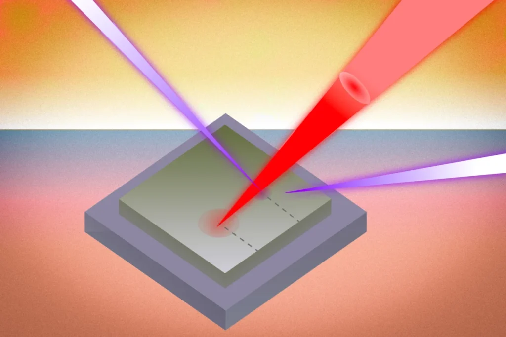
The methodology developed by the MIT researchers, in collaboration with scientists at the Argonne National Laboratory and the University of Texas at Austin, leverages an emerging analysis technique known as ultrafast X-ray diffraction. The process begins by hitting a sample material with a laser pulse, which acts as a localized heat source. Simultaneously, the researchers fire pulses of high-intensity X-rays at the material.
As the laser heats the sample, the atoms within the material vibrate and the crystal lattice expands. These subtle physical changes, known as material strain, alter the way the X-rays diffract when they pass through the device. By measuring these diffraction patterns in real-time, the researchers can calculate the exact temperature and heat flow at specific points within the multilayered stack.
"Over the last few years, researchers have developed what is basically the brightest X-ray source in the world," said Thanh Nguyen, a PhD graduate from MIT and co-lead author of the paper. This refers to the advanced synchrotron facilities, such as those at Argonne National Laboratory, which provide the high-flux X-ray beams necessary for such precise measurements. "That allows you to focus an X-ray beam and get incredibly fine spatial resolution. You can also use a laser to heat the sample while the X-ray scans and shows how the heat dissipates across space in real-time."
Experimental Findings: The Impact of Micro-Defects
To test the efficacy of the system, the researchers applied the technique to a device consisting of a layer of gallium nitride (GaN) grown on a silicon substrate. GaN is a wide-bandgap semiconductor that is highly prized for its high thermal conductivity and its ability to handle high voltages, making it a staple in 5G infrastructure, electric vehicle power converters, and advanced radar systems.
Despite its potential, GaN devices often underperform in real-world settings due to defects introduced during the manufacturing process. Using their X-ray technique, the MIT team identified a single "wrinkle" defect—a micron-scale structural imperfection—within the GaN layer. The results were startling: the defect caused a fourfold (400%) reduction in the material’s ability to transfer heat at that specific location. Furthermore, the researchers observed that the defect caused heat to spread anisotropically, meaning it moved more easily in one direction than the other, leading to "hotspots" that could eventually degrade the device’s integrity.
"When people model heat dissipation, they model perfect crystals without defects," said Mingda Li, an associate professor of nuclear science and engineering at MIT. "But these types of large wrinkle defects are very common in 2D materials. People never even knew how much heat is blocked by these wrinkles. Those are things we can now directly observe with this technique."
Chronology of Development and Collaborative Efforts
The development of this technique is the culmination of several years of interdisciplinary research. The timeline of this breakthrough reflects the growing necessity for specialized thermal diagnostics in the semiconductor roadmap:
- 2018–2021: Early conceptualization of using synchrotron radiation for thermal mapping in semiconductors began, following the increased availability of ultrafast X-ray pulses.
- 2022: The research team focused on Gallium Nitride, recognizing its critical role in the next generation of power electronics. Preliminary tests indicated that traditional optical methods were providing incomplete data on GaN-on-Silicon interfaces.
- 2023: Collaboration with Argonne National Laboratory allowed the team to utilize world-class X-ray diffraction facilities to refine the spatial resolution of the measurements to the nanometer scale.
- 2024: The team successfully quantified the thermal impact of localized defects, leading to the publication of their findings in Nature Communications.
The study involved a massive collaborative effort, including researchers from MIT’s Department of Nuclear Science and Engineering, the Department of Mechanical Engineering, and the Research Laboratory of Electronics, as well as experts from the University of Texas at Austin and the Argonne National Laboratory.
Industry Implications and Future Outlook
The semiconductor industry has already taken note of the MIT team’s work. According to Professor Li, a leading semiconductor industry consortium has already reached out to discuss applying this measurement technique to commercial chip architectures. The ability to perform these "thermal biopsies" on active devices allows companies to move beyond theoretical modeling and base their designs on empirical data.
The implications for this technology extend across several high-growth sectors:
- Artificial Intelligence: AI accelerators and GPUs generate immense heat. Understanding how to better vent this heat from 3D-stacked memory (HBM) and logic units could lead to more stable and faster AI hardware.
- Electric Vehicles (EVs): Power modules in EVs rely on GaN and Silicon Carbide (SiC) to manage high currents. Reducing thermal resistance in these modules can improve vehicle range and charging speeds.
- Consumer Wearables: In devices like smartwatches or augmented reality (AR) glasses, there is no room for cooling fans. Efficient passive heat dissipation is essential for user comfort and battery longevity.
- Clean Energy: High-efficiency solar inverters and grid-scale power converters require robust thermal management to operate continuously for decades.
"Chip developers need devices that can handle heat," Mingda Li noted. "I think overheating has become the real bottleneck in device performance. Eventually, they’d like to go beyond that to study the heat carriers and understand exactly what causes failure, in order to avoid local hotspots and design better devices. This approach is a step in that direction."
Analysis of Broader Impact
The success of this X-ray-based diagnostic tool marks a shift in semiconductor research from a focus on purely electrical characteristics to a holistic view of "electro-thermal" performance. As the industry approaches the physical limits of Moore’s Law, the "More than Moore" strategy—which involves 3D integration and heterogeneous chiplets—will rely heavily on the thermal insights provided by this technique.
Furthermore, the discovery of how significantly a single micro-defect can disrupt heat flow suggests that manufacturing yields and device reliability could be improved by refining the growth processes of thin-film materials. By identifying the specific types of wrinkles or dislocations that are most detrimental to heat flow, manufacturers can optimize their fabrication pipelines to minimize these specific flaws.
The research was supported by a diverse array of funding bodies, including the U.S. Department of Energy, the U.S. National Science Foundation, and the MIT School of Engineering. As the team continues to refine the method, they hope to make it more accessible for industrial applications, potentially integrating similar diagnostic capabilities into high-throughput quality control systems for the next generation of microelectronics.