In a landmark development for the field of quantum materials science, a multidisciplinary team of researchers at the Massachusetts Institute of Technology (MIT) and several partner institutions has successfully engineered a method to produce and integrate air-stable, monolayer-thick superconductors at a wafer-scale. This breakthrough, recently published in the journal Nature, addresses one of the most persistent hurdles in quantum hardware engineering: the extreme fragility and atmospheric sensitivity of two-dimensional (2D) superconducting materials. By growing these materials underneath a protective layer of graphene, the team has not only demonstrated a path toward the miniaturization of quantum circuits but has also unlocked new possibilities for the mass production of high-performance quantum detectors and communication technologies.
The research focuses on niobium diselenide (NbSe2), an ultrathin superconductor that consists of a single layer of niobium atoms sandwiched between two layers of selenium atoms. While the material has long been recognized for its extraordinary electronic properties, its tendency to oxidize and degrade almost instantly upon exposure to air has previously relegated it to controlled laboratory environments and small-scale experimentation. The new process developed at MIT allows for the creation of smooth, continuous films of NbSe2 over an inch in size—a scale that is compatible with modern semiconductor manufacturing processes.
The Evolution of Two-Dimensional Superconductivity
Superconductors are a class of materials capable of conducting electricity with zero energy loss. In the realm of quantum computing, they are indispensable for creating qubits—the fundamental building blocks of quantum information—and the circuitry that interconnects them. However, traditional superconducting components are often bulky, posing a significant challenge as engineers attempt to scale quantum systems from a few dozen qubits to the thousands or millions required for practical applications.
The emergence of 2D materials, which are only a few atoms thick, offered a theoretical solution to this "scaling bottleneck." Niobium diselenide, in particular, is valued for its high kinetic inductance. Kinetic inductance is a quantum mechanical phenomenon where the inertia of charge carriers (Cooper pairs) allows the material to store magnetic energy. Because NbSe2 can store a high amount of inductive energy in an incredibly small physical footprint, it is an ideal candidate for replacing large arrays of Josephson junctions—complex electronic components currently used to provide inductance in quantum circuits. By replacing these arrays with a single, tiny film of NbSe2, engineers can drastically reduce the size of quantum hardware.
Overcoming the "Atmospheric Barrier"
Despite the potential of NbSe2, the practical application of the material has been stymied by its chemical instability. Historically, researchers have relied on the "exfoliation" method—popularly known as the "Scotch tape method"—to peel small flakes of the material from a bulk crystal. While useful for basic research, this method produces irregular, microscopic samples that cannot be integrated into industrial-scale electronics. Furthermore, because NbSe2 is highly reactive, it begins to oxidize the moment it is removed from the inert vacuum chambers where it is synthesized.
"Typically, once we make the material and remove it from its inert environment, it immediately starts to oxidize and degrade, ultimately becoming damaged," explained Xudong Sheldon Zheng, a graduate student in the MIT Department of Electrical Engineering and Computer Science (EECS) and co-lead author of the study.
Previous attempts to protect the material involved "capping" it with other 2D materials like hexagonal boron nitride or graphene after the growth process was complete. However, even the briefest exposure during the transfer process was often enough to compromise the superconductor’s integrity. The MIT team realized that for the material to be viable, the protection had to be integrated into the growth process itself.
The Innovation: Growth Under the "Graphene Blanket"
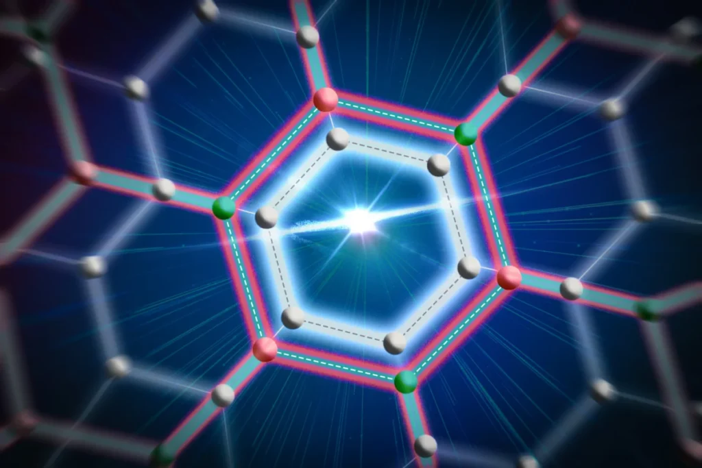
The core of the researchers’ innovation lies in a technique they describe as growing the material in a "tiny gap." Instead of growing the superconductor on a substrate and then trying to cover it, the team first placed a layer of graphene onto a silicon dioxide substrate. Using chemical vapor deposition (CVD), they then introduced the precursors for niobium diselenide.
In a surprising discovery, the researchers found that the precursors could migrate into the sub-nanometer space between the graphene and the silicon dioxide. The weak van der Waals forces that hold the graphene to the substrate leave a gap of less than one nanometer. Within this confined space, the NbSe2 crystal begins to form. The silicon dioxide acts as a template to trap the precursors, while the graphene layer acts as a flexible "blanket" that allows the material to spread out into a continuous, uniform monolayer while simultaneously shielding it from the atmosphere.
"It took a long time for us to understand how the growth could happen underneath the graphene," Zheng noted. "Through collaboration and discussion, we eventually uncovered the mechanism for growing the material at the interface, and this solves a lot of problems and allows us to simplify our fabrication steps."
Technical Validation and Circuit Integration
To prove the utility of this "encapsulated-at-birth" superconductor, the team integrated the NbSe2-graphene structure into a superconducting microwave circuit. This required overcoming another significant engineering hurdle: establishing a reliable electrical connection between a 1-nanometer-thick film and traditional electrodes that are several hundred nanometers thick.
Sameia Zaman, an EECS graduate student and co-lead author, explained the difficulty: "It is challenging to make a good electrical connection between this very thin material and our electrodes." To solve this, the team employed a specialized vacuum etching process to create "side-wall" contacts. By etching the edges of the NbSe2-graphene stack in a vacuum, they were able to preserve the clean, unoxidized edge of the superconductor, allowing for a robust electrical interface with the rest of the circuit.
Testing confirmed that the material maintained its superconducting properties throughout the fabrication process. Most importantly, it exhibited the high kinetic inductance necessary for quantum device applications. This marks the first time that a monolayer superconductor has been grown at a wafer scale and integrated into a functional circuit without losing its performance due to environmental degradation.
Collaborative Effort and Institutional Support
The research was a massive collaborative undertaking involving experts in physics, electrical engineering, and materials science. Joining Zheng and Zaman as co-lead authors was Kenan Zhang, a former postdoc in the MIT Research Laboratory of Electronics (RLE). The project was guided by corresponding authors William D. Oliver, a professor of physics and EECS at MIT; Jing Kong, the Jerry McAfee Professor in Engineering at MIT; and Joel Wang, an assistant professor at New York University.
The study also included contributions from researchers at the MIT Lincoln Laboratory, Rice University, Yale University, and Pohang University of Science and Technology in South Korea. This international and interdisciplinary approach was essential for bridging the gap between fundamental materials science and practical device engineering.
The research was supported by a wide array of funding bodies, reflecting the strategic importance of quantum materials. Sponsors included the U.S. Army Research Office, the National Science Foundation, the Department of Energy, and the Air Force Office of Scientific Research, among others. Much of the fabrication work was conducted at the MIT.nano facility, a state-of-the-art laboratory designed for the manipulation of materials at the nanoscale.
Broader Implications for Quantum Technology
The ability to produce air-stable, 2D superconductors at scale has implications that extend far beyond the laboratory.
- Hardware Miniaturization: Current superconducting quantum computers, such as those being developed by IBM and Google, require massive dilution refrigerators to keep their bulky circuits at near-absolute zero temperatures. By using 2D materials with high kinetic inductance, engineers can design much more compact circuits, potentially allowing for higher qubit densities on a single chip.
- Quantum Sensing and Cosmology: The high sensitivity of NbSe2 makes it an excellent candidate for ultra-sensitive quantum detectors. These could be used in telecommunications to detect extremely faint signals or in cosmology to observe the cosmic microwave background radiation with unprecedented precision.
- Fundamental Physics: For scientists, the ability to grow large, uniform samples of monolayer superconductors provides a new "playground" for studying exotic physics, such as Ising superconductivity and the transition between 2D and 3D electronic states.
- Universal Growth Strategy: The MIT team demonstrated that their "under-the-graphene" growth strategy is not limited to NbSe2. It can be applied to an entire family of transition metal dichalcogenides (TMDs) and other monolayer quantum materials, paving the way for a new era of "protected" 2D electronics.
Conclusion and Future Outlook
The transition from "small flakes" to "wafer-scale" production marks a pivotal moment in the timeline of 2D materials. By solving the dual problems of scalability and atmospheric degradation, the MIT-led team has moved monolayer superconductors out of the realm of scientific curiosity and into the realm of industrial potential.
"We’ve taken a very good step toward exploring both the physics and the application side of this thin, monolayer superconductor," said Sameia Zaman. "There are a lot of directions we can go in the future."
The researchers now plan to refine the process further, exploring how these materials can be stacked to create even more complex "van der Waals heterostructures." As the global race for quantum supremacy intensifies, the ability to manufacture stable, ultra-compact superconducting components may prove to be the decisive factor in bringing quantum computers out of the lab and into the real world.