A significant hurdle in the global race to develop practical quantum technologies has been addressed by researchers at Stanford University, who have engineered a nanoscale optical device capable of operating at room temperature while effectively linking the quantum properties of light and electrons. This breakthrough directly confronts one of the most persistent and costly challenges in quantum computing and communication: the necessity for temperatures near absolute zero, approximately -459 degrees Fahrenheit, to maintain the fragile quantum states essential for computation and information transfer. The development holds profound implications for the future of quantum systems, promising smaller, more affordable, and more widely deployable quantum technologies, particularly for transmitting information across long distances without the prohibitive infrastructure currently required.
The Cryogenic Conundrum: A Hurdle for Quantum’s Promise
For decades, the promise of quantum computing has been tantalizingly out of reach for widespread application, largely due to the extreme environmental conditions its delicate components demand. Quantum computers harness phenomena like superposition and entanglement to process information in fundamentally different ways than classical computers. However, these quantum states are incredibly fragile, susceptible to even the slightest environmental interference, a phenomenon known as decoherence. To combat this, most leading quantum computing architectures, such as superconducting qubits used by giants like IBM and Google, require elaborate cryogenic cooling systems. These systems often involve multiple stages of dilution refrigerators, bringing temperatures down to millikelvin ranges – colder than deep space.
This requirement for extreme cold translates into enormous operational costs, significant energy consumption, and immense physical footprints for quantum machines. A single dilution refrigerator can be as large as a small car and consume substantial power, making quantum computing facilities complex, expensive, and inaccessible to all but the most well-funded research institutions and corporations. The sheer engineering challenge of maintaining these ultra-low temperatures has been a primary bottleneck, limiting scalability and practical integration of quantum components into existing technological infrastructures. The pursuit of "hot qubits" – quantum systems that can operate at warmer temperatures – has thus become a holy grail for quantum researchers worldwide.
Stanford’s Room-Temperature Revelation: A Nanoscale Solution
The Stanford team’s innovation directly addresses this cryogenic challenge by demonstrating a device that achieves a fundamental quantum connection at ambient temperatures. At its core, the device facilitates entanglement between photons, the elementary particles of light, and electrons, the carriers of electric charge. This ability to create a stable, room-temperature quantum link between light and matter is considered a foundational requirement for building future quantum communication networks, often envisioned as a "quantum internet."
"The material in question is not really new, but the way we use it is," explains Jennifer Dionne, a professor of materials science and engineering at Stanford and the senior author of the study published in Nature Communications. "It provides a very versatile, stable spin connection between electrons and photons that is the theoretical basis of quantum communication. Typically, however, the electrons lose their spin too quickly to be useful." This statement underscores the critical nature of the stability achieved by the Stanford device, overcoming a persistent problem in quantum material science.
-
Unpacking the Device: MoSe2 and Silicon Nanostructures.
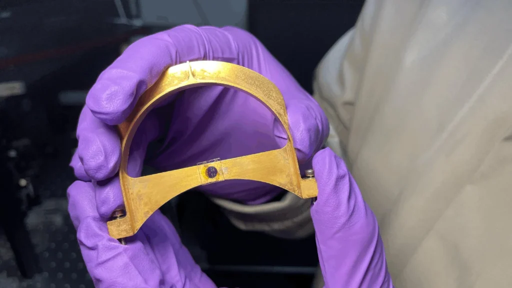
The device itself is a marvel of nanoscale engineering, combining a thin, patterned layer of molybdenum diselenide (MoSe2) with a nanopatterned silicon substrate. Molybdenum diselenide belongs to a class of materials known as transition metal dichalcogenides (TMDCs), which have garnered significant scientific interest in recent years due to their unique optical and quantum properties. These materials exhibit strong light-matter interaction and spin-valley coupling, making them prime candidates for next-generation optoelectronic and quantum devices. The collaboration with Stanford researchers Fang Liu and Tony Heinz, specialists in TMDC materials, was instrumental in harnessing these properties effectively. -
The Magic of "Twisted Light" and Spin Impartation.
A crucial element of the device’s functionality lies in the silicon nanostructures. These structures are not merely passive supports; they actively manipulate light in a sophisticated manner, generating what the researchers term "twisted light." Feng Pan, a postdoctoral scholar in Dionne’s lab and the paper’s first author, elaborated on this: "The Silicon nanostructures enable what we call ‘twisted light.’ The photons spin in a corkscrew fashion, but more importantly, we can use these spinning photons to impart spin on electrons that are the heart of quantum computing."This concept of "twisted light" refers to photons carrying orbital angular momentum (OAM), where the wavefronts twist around the beam axis like a corkscrew. While the fundamental spin of a photon relates to its polarization, OAM adds another degree of freedom, allowing for more complex encoding of information. The patterned nanostructures, imperceptible to the human eye due to their size being comparable to visible light wavelengths, are engineered with exquisite precision to achieve this manipulation. "The patterned nanostructures are imperceptible to the human eye, about the size of the wavelength of visible light," Dionne adds. "But they help us manipulate photons very precisely to make them spin — to twist them — in a specific direction, for example, up or down." This precise control over photon OAM is key to efficiently transferring quantum information (spin) to electrons, establishing the entanglement necessary for quantum operations.
A New Paradigm for Quantum Communication
The ability to create stable entanglement between twisted light and electron spins at room temperature directly addresses one of the biggest challenges in quantum information science: maintaining stable quantum states and efficiently transmitting them. In conventional computing, information is represented by bits, which are either 0 or 1. Quantum technologies utilize qubits, which can exist in a superposition of 0 and 1 simultaneously, and can be entangled with other qubits, enabling entirely new paradigms for processing and transmitting information.
-
Bridging the Gap: Photons, Electrons, and the Quantum Internet.
The device’s capacity to entangle photons and electrons is particularly significant for quantum communication. Photons are ideal for transmitting quantum information over distances because they travel at the speed of light and interact minimally with their environment. However, for storage and processing, matter-based qubits (like electron spins) are often preferred due to their longer coherence times and ability to be manipulated within a quantum processor. This device acts as a crucial interface, allowing quantum information to be transferred from robust, stationary electron qubits to mobile photonic qubits and vice versa, without the need for cryogenic interfaces. This could be a foundational component for quantum repeaters and quantum memory nodes in a future quantum internet, which aims to enable secure communication and distributed quantum computing across geographically separated nodes. -
Overcoming Distance and Environmental Interference.
The current limitations of quantum communication largely stem from photon loss in optical fibers and the difficulty of maintaining entanglement over long distances. While quantum key distribution (QKD) is already commercially available, it typically relies on line-of-sight or short fiber links, or requires complex, bulky satellite systems for intercontinental communication. Room-temperature, stable entanglement devices could simplify the design of quantum repeaters, which are essential for extending the range of quantum networks by periodically "refreshing" and re-entangling quantum signals, much like classical repeaters boost optical signals. By operating at room temperature, these repeaters could be significantly smaller, cheaper, and easier to deploy in existing fiber optic infrastructure or even in less controlled environments, potentially accelerating the deployment of a global quantum communication infrastructure.
The Material Science at the Core: Why TMDCs Matter
The choice of molybdenum diselenide (MoSe2) as the active material is far from arbitrary. Transition metal dichalcogenides (TMDCs) are 2D materials, similar in concept to graphene, but with distinct electronic and optical properties that make them exceptionally well-suited for quantum applications. Unlike graphene, many TMDCs have a direct bandgap, meaning they can efficiently absorb and emit light. They also exhibit strong spin-orbit coupling, which links an electron’s spin to its momentum, and pronounced excitonic effects, where electrons and holes (missing electrons) form bound pairs called excitons that can be readily manipulated by light. These properties enable robust interaction between light and electron spins, which is precisely what the Stanford device leverages.
"It all comes down to this material and our Silicon chip," Pan emphasizes. "Together, they efficiently confine and enhance the twisting of light to create a strong coupling of spin between photons and electrons. This stabilizes the quantum state that makes quantum communication possible." The ability to create a strong light-matter interaction within a stable quantum state at room temperature distinguishes this work from many previous attempts, which often struggled with the rapid decoherence of electron spins at higher temperatures.
- A Legacy of Innovation: Jennifer Dionne’s Vision.
Professor Jennifer Dionne’s lab at Stanford has a long-standing reputation for pioneering work in nanophotonics and plasmonics, focusing on manipulating light at the nanoscale to unlock new functionalities. This latest breakthrough is a testament to her group’s expertise in materials science and engineering, particularly in designing metasurfaces and nanostructures that can control light with unprecedented precision. The integration of advanced material science with sophisticated nanophotonic design is a hallmark of this research, pushing the boundaries of what is possible in quantum device engineering.
Economic and Energy Implications: Making Quantum Accessible
Beyond the fundamental scientific achievement, the practical implications of a room-temperature quantum device are vast, particularly concerning the economic viability and energy footprint of quantum technologies.
-
Reducing the Footprint: Cost and Energy Efficiency.
Current quantum computing systems, reliant on cryogenic cooling, are notoriously expensive to build, operate, and maintain. The infrastructure alone can cost millions of dollars, and the energy consumption for cooling can be substantial. For instance, large-scale superconducting quantum processors might require tens to hundreds of kilowatts of power, much of it dedicated to maintaining ultra-low temperatures. A room-temperature device eliminates the need for these elaborate and energy-intensive cooling systems, drastically reducing both the capital expenditure and operational costs. This cost reduction could democratize access to quantum technologies, moving them from specialized, climate-controlled bunkers to potentially more ubiquitous settings. -
The Path to Miniaturization and Widespread Adoption.
The compact, nanoscale design of the Stanford device also presents a clear pathway toward miniaturization. Without the bulky cryogenic apparatus, quantum components could be integrated into much smaller form factors. This opens up possibilities for quantum sensors in mobile devices, quantum communication nodes in urban infrastructure, or even distributed quantum computing clusters that are far more practical to deploy than current setups. The ability to operate at room temperature also simplifies integration with existing classical electronic components, fostering a hybrid quantum-classical computing environment that many foresee as the immediate future of quantum technology. Analysts and industry experts often point to miniaturization and cost reduction as critical factors for quantum technology to move beyond the laboratory and into mainstream commercial and industrial applications.
Broader Horizons: Impact Across Industries
If further developed and scaled, this technology could catalyze advancements across a multitude of sectors, from secure communications to artificial intelligence and drug discovery.
-
Secure Communications and Quantum Key Distribution (QKD).
The most immediate and apparent impact would be on secure communication. Quantum Key Distribution (QKD) already offers theoretically unbreakable encryption based on the laws of quantum mechanics. However, current QKD systems are limited by distance and require dedicated fiber optic lines or satellite links. Room-temperature entanglement devices could enable more robust, long-distance QKD networks, potentially forming the backbone of a truly secure quantum internet resistant to even future quantum computer-based attacks. Governments and defense organizations worldwide are heavily investing in quantum-secure communication, and this breakthrough could significantly accelerate their efforts. -
AI, Drug Discovery, and Complex Simulations.
Beyond communication, the implications for computing are equally profound. While this specific device is focused on light-matter entanglement for communication, the underlying principles of stable, room-temperature qubits could eventually influence quantum computing architectures. Quantum computers hold the potential to revolutionize fields like artificial intelligence by enabling faster training of complex models and solving optimization problems currently intractable for classical computers. In drug discovery and materials science, quantum simulations could accurately model molecular interactions at an atomic level, leading to the development of new medicines, catalysts, and advanced materials with unprecedented properties. Financial modeling, logistics optimization, and climate science also stand to benefit from the enhanced computational power of quantum systems.
The Global Quantum Race: Contextualizing the Breakthrough
The Stanford breakthrough arrives amidst an intense global race to achieve quantum supremacy and establish leadership in quantum technologies. Nations like the United States, China, and member states of the European Union, along with tech giants such as IBM, Google, Microsoft, and Amazon, are investing billions in quantum research and development. This competition spans various quantum modalities, including superconducting qubits, trapped ions, photonic qubits, and topological qubits, each with its own advantages and challenges.
The development of room-temperature quantum components is a critical front in this race. While significant progress has been made in increasing the number of qubits in cryogenic systems, the inherent infrastructure limitations continue to pose a barrier to widespread adoption. Breakthroughs like Stanford’s, which address fundamental operational constraints, are highly valued as they could shift the technological landscape and accelerate the timeline for practical quantum applications. This research will undoubtedly draw significant attention from international research communities and funding bodies seeking pathways to more deployable quantum solutions.
The Road Ahead: Scaling and Integration
The researchers are not resting on their laurels. The immediate next steps involve continuing to improve the device’s performance, exploring additional TMDC materials and combinations that could offer even greater stability and efficiency, and investigating whether these systems might reveal new quantum capabilities not currently possible at room temperature.
-
From Lab to Network: Building the Quantum Future.
A longer-term, yet crucial, goal is the integration of these nanoscale devices into larger quantum networks. Achieving this vision will necessitate parallel advancements in supporting technologies, including more efficient quantum light sources, high-speed modulators, sensitive detectors, and robust interconnects that can seamlessly link multiple quantum components. The journey from a proof-of-concept laboratory device to a fully functional quantum network is arduous, requiring concerted efforts across multiple scientific and engineering disciplines. -
The Cell Phone Quantum Dream.
Ultimately, the grand vision for quantum technology includes miniaturizing components to such an extent that they could be incorporated into everyday electronics. While this future remains many years, if not decades, away, the work by the Stanford team represents a concrete and significant step toward making quantum technology more accessible and practical for a broader range of applications. Pan’s hopeful outlook captures this ambition: "If we can do that, maybe someday we could do quantum computing in a cell phone. But that’s a 10-plus-year plan." This aspiration, though distant, underscores the transformative potential of such fundamental advancements in quantum material science and engineering, moving quantum from the realm of esoteric physics to a future ubiquitous technology.